SLVS727E November 2006 – October 2019 TPS2410 , TPS2411
PRODUCTION DATA.
- 1 Features
- 2 Applications
- 3 Description
- 4 Revision History
- 5 Device Comparison
- 6 Pin Configuration and Functions
- 7 Specifications
- 8 Detailed Description
- 9 Application and Implementation
- 10Power Supply Recommendations
- 11Layout
- 12Device and Documentation Support
- 13Mechanical, Packaging, and Orderable Information
Package Options
Mechanical Data (Package|Pins)
Thermal pad, mechanical data (Package|Pins)
Orderable Information
9.2.4.1 MOSFET Selection and R(RSET)
MOSFET selection criteria include voltage rating, voltage drop, power dissipation, size, and cost. The voltage rating consists of both the ability to withstand the rail voltage with expected transients, and the gate breakdown voltage. The MOSFET gate rating should be the minimum of 12 V or the controlled rail voltage. Typically this requires a ±20 V GATE voltage rating.
While rDS(on) is often chosen with the power dissipation, voltage drop, size and cost in mind, there are several other factors to be concerned with in ORing applications. When using the TPS2410, the minimum voltage across the device is 10 mV. A device that would have a lower voltage drop at full-load would be over-specified. When using a TPS2411 or TPS2410 with RSET programmed to a negative voltage, the permitted static reverse current is equal to the turn-off threshold divided by the rDS(on). While this current may actually be desirable in some systems, the amount may be controlled by selection of rDS(on) and RSET. The practical range of rDS(on) runs from the low milliohms to 40 mΩ for a single MOSFET.
MOSFETs may be paralleled for lower voltage drop (power loss) at high current. For TPS2410 operation, one should plan for only one of the MOSFETs to carry current until the 10 mV regulation point is exceeded and the loop forces GATE fully ON. TPS2411 operation does not rely on linear range operation, so the MOSFETs are all ON or OFF together except for short transitional times. Beyond the control issues, current sharing depends on the resistance match including both the rDS(on) and the connection resistance.
The TPS2410 may be used without a resistor on RSET If the turnoff V(AC) threshold is about 3 mV. The TPS2411 may only be operated without an RSET programming resistor if the loading provides a higher V(AC). A larger negative turnoff threshold reduces sensitivity to false tripping due to noise on the bus, but permits larger static reverse current. Installing a resistor from RSET to ground creates a negative shift in the fast turn-off threshold per Equation 3.

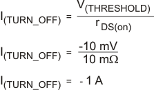
To obtain a –10 mV fast turnoff ( V(A) is less than V(C) by 10 mV ), R(RSET) = (–470.02/ ( –0.01–0.00314) ) ≈ 35,700Ω. If a 10 mΩ rDS(on) MOSFET was used, the reverse turnoff current is calculated as follows.

The sign indicates that the current is reverse, or flows from the MOSFET drain to source ( C to A ).
The turn-off speed of a MOSFET is influenced by the effective gate-source and gate-drain capacitance (CISS). Since these capacitances vary a great deal between different vendor parts and technologies, they should be considered when selecting a MOSFET where the fastest turn-off is desired.