SLVS727E November 2006 – October 2019 TPS2410 , TPS2411
PRODUCTION DATA.
- 1 Features
- 2 Applications
- 3 Description
- 4 Revision History
- 5 Device Comparison
- 6 Pin Configuration and Functions
- 7 Specifications
- 8 Detailed Description
- 9 Application and Implementation
- 10Power Supply Recommendations
- 11Layout
- 12Device and Documentation Support
- 13Mechanical, Packaging, and Orderable Information
Package Options
Mechanical Data (Package|Pins)
Thermal pad, mechanical data (Package|Pins)
Orderable Information
8.4.1 TPS2410 vs TPS2411 – MOSFET Control Methods
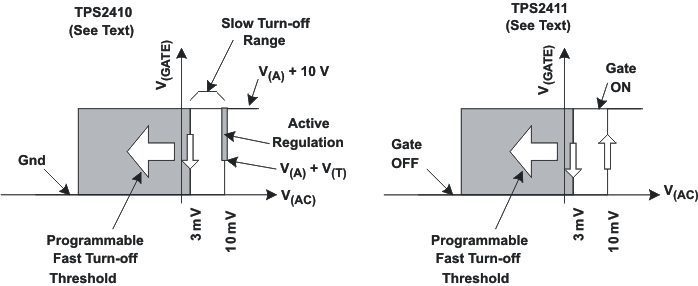
The TPS2410 turns the MOSFET on with a linear control loop that regulates V(AC) to 10 mV as shown in Figure 9. With the gate low, and V(AC) increasing to 10 mV, the amplifier drives GATE high with all available output current until regulation is reached. The regulator controls V(GATE) to maintain V(AC) at 10 mV as long as the MOSFET rDS(on) × I(DRAIN) is less than this the regulated voltage. The regulator drives GATE high, turning the MOSFET fully ON when the rDS(on) × I(DRAIN) exceeds 10 mV; otherwise, V(GATE) is near V(A) plus the MOSFET gate threshold voltage. If the external circuits force V(AC) below 10 mV and above the programmed fast turnoff, GATE is slowly turned off. GATE is rapidly pulled to ground if V(AC) falls to the RSET programmed fast turn-off threshold.
The TPS2411 turns the MOSFET on and off like a comparator with hysteresis as shown in Figure 9. GATE is driven high when V(AC) exceeds 10 mV, and rapidly turned off if V(AC) falls to the RSET programmed fast turn-off threshold.
System designs should account for the inherent delay between a device circuit becoming forward biased, and the MOSFET actually turning ON. The delay is the result of the MOSFET gate capacitance charge from ground to its threshold voltage by the 270 μA gate current. If there are no additional sources holding the ORed rail voltage up, the MOSFET internal diode conductd and maintain voltage on the ORed output, but there is some voltage droop. This condition is analogous to the power source being ORed in this case. The DC/DC converter output voltage droops when its load increases from zero to a high value. Load sharing techniques that keep all ORed sources active solve this condition.
 Figure 9. TPS2410, TPS2411 Operation
 The operation of the two parts is summarized in Table 1.
Table 1. Operation as a Function of VAC
| V(AC) ≤ Turnoff Threshold(1) | Turnoff Threshold(1) ≤ VAC ≤ 10 mV | V(AC) > 10 mV | ||
|---|---|---|---|---|
| V(AC) Forced < 10 mV | (MOSFET
rDS(on) × ILOAD) ≤ 10 mV |
|||
| TPS2410 | Strong GATE pull-down (OFF) | Weak GATE pull-down (OFF) | V(AC) regulated to 10 mV | GATE pulled high (ON) |
| TPS2411 | Strong GATE pull-down (OFF) | Depends on previous state (Hysteresis region) | GATE pulled high (ON) | |
The TPS2410 control method yields several benefits. First, the low current GATE driver provides a gentle turn-on and turn-off for slowly rising and falling input voltage. Second, it reduces the tendency for on/off cycling of a comparator based solution at light loads. Third, it avoids reverse currents if the fast turn-off threshold is left positive. The drawback to this method is that the MOSFET appears to have a high resistance at light load when the regulation is active. A momentary output voltage droop occurs when a large step load is applied from a light-load condition. The TPS2410 is a better solution for a mid-rail bus that is re-regulated.
The TPS2411 turns the MOSFET on if V(AC) is greater than 10 mV, and hard off when V(AC) is less than the RSET programmed threshold. There is no linear control range and slow turn-off. The disadvantage is that the turn-off threshold must be negative (unless a specified load is always present) permitting a continuous reverse current. Under a dynamic reverse voltage fault, the lower threshold voltage may permit a higher peak reverse current. There are a number of advantages to this control method. Step loads from a light load condition are handled without a voltage droop beyond I × R. If the redundant converter fails, applications with redundant synchronous converters may permit a small amount of reverse current at light load in order to assure that the MOSFET is all ready on. The TPS2411 is a better solution for low-voltage busses that are not re-regulated, and that may see large load steps transients.
These applications recommendations are meant as a starting point, with the needs of specific implementations over-riding them.