SLVS727E November   2006  – October 2019 TPS2410 , TPS2411

PRODUCTION DATA.  

  1. Features
  2. Applications
  3. Description
    1.     Device Images
      1.      Typical Application Diagram
  4. Revision History
  5. Device Comparison
  6. Pin Configuration and Functions
    1.     Pin Functions, PW
    2.     Pin Functions, RMS
  7. Specifications
    1. 7.1 Absolute Maximum Ratings
    2. 7.2 ESD Ratings
    3. 7.3 Recommended Operating Conditions
    4. 7.4 Thermal Information
    5. 7.5 Electrical Characteristics: TPS2410, 11
    6. 7.6 Typical Characteristics
  8. Detailed Description
    1. 8.1 Overview
    2. 8.2 Functional Block Diagram
    3. 8.3 Feature Description
      1. 8.3.1 Device Pins
        1. 8.3.1.1  A, C:
        2. 8.3.1.2  BYP:
        3. 8.3.1.3  FLTR:
        4. 8.3.1.4  FLTB:
        5. 8.3.1.5  GATE:
        6. 8.3.1.6  GND:
        7. 8.3.1.7  RSET:
        8. 8.3.1.8  RSVD:
        9. 8.3.1.9  STAT
        10. 8.3.1.10 UV, OV, PG:
        11. 8.3.1.11 VDD:
      2. 8.3.2 Gate Drive, Charge Pump and C(BYP)
      3. 8.3.3 Fast Comparator Input Filtering – C(FLTR)
      4. 8.3.4 UV, OV, and PG
      5. 8.3.5 Input ORing and Stat
    4. 8.4 Device Functional Modes
      1. 8.4.1 TPS2410 vs TPS2411 – MOSFET Control Methods
  9. Application and Implementation
    1. 9.1 Typical Connections
      1. 9.1.1 N+1 Power Supply
      2. 9.1.2 Input ORing
    2. 9.2 Typical Application Examples
      1. 9.2.1 VDD, BYP, and Powering Options
      2. 9.2.2 Bidirectional Blocking and Protection of C
      3. 9.2.3 ORing Examples
      4. 9.2.4 Design Requirements
        1. 9.2.4.1 MOSFET Selection and R(RSET)
        2. 9.2.4.2 TPS2410 Regulation-loop Stability
      5. 9.2.5 Detailed Design Procedure
      6. 9.2.6 Application Curves
  10. 10Power Supply Recommendations
    1. 10.1 Recommended Operating Range
    2. 10.2 System Design and Behavior with Transients
  11. 11Layout
    1. 11.1 Layout Considerations
    2. 11.2 Layout Example
  12. 12Device and Documentation Support
    1. 12.1 Device Support
    2. 12.2 Related Links
    3. 12.3 Receiving Notification of Documentation Updates
    4. 12.4 Community Resources
    5. 12.5 Trademarks
    6. 12.6 Electrostatic Discharge Caution
    7. 12.7 Glossary
  13. 13Mechanical, Packaging, and Orderable Information

Package Options

Mechanical Data (Package|Pins)
Thermal pad, mechanical data (Package|Pins)
Orderable Information

UV, OV, and PG

The UV and OV inputs can be used in a several ways. These include voltage monitoring and forcing the pass MOSFET off.

A voltage bus may be monitored for undervoltage with the UV pin, and overvoltage with the OV pin. Figure 7 demonstrates a basic three resistor divider, however, two separate two resistor dividers may be used. PG is high if V(UV) exceeds the UV threshold, and V(OV) is below the OV threshold, else PG is low. Each of these inputs has a 0.6-V threshold and 7 mV of hysteresis. Optionally, UV and OV may be independently disabled by connecting them to ground, and PG may be left floating if not used. The state of PG is undefined until the internal UVLO is satisfied.

GATE is forced low if V(OV) exceeds 0.6 V. This allows OV to be used as an enable as shown in Figure 7. This can be used for testing purposes, or control of back-to-back MOSFETs to force an output off even though V(AC) is greater than 10 mV.
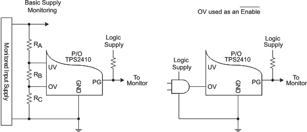
TPS2410 TPS2411 pwr_opt_lvs727.gifFigure 7. UV, OV, AND PG