SLVSC87C October 2013 – December 2018 TPS24750 , TPS24751
UNLESS OTHERWISE NOTED, this document contains PRODUCTION DATA.
- 1 Features
- 2 Applications
- 3 Description
- 4 Revision History
- 5 Device Comparison Table
- 6 Pin Configuration and Functions
- 7 Specifications
- 8 Parameter Measurement Information
-
9 Detailed Descriptions
- 9.1 Overview
- 9.2 Functional Block Diagram
- 9.3 Feature Description
- 9.4 Device Functional Modes
-
10Application and Implementation
- 10.1 Application Information
- 10.2
Typical Application
- 10.2.1 Design Requirements
- 10.2.2
Detailed Design Procedure
- 10.2.2.1
Power-Limited Start-Up
- 10.2.2.1.1 STEP 1. Choose RSENSE, RSET, and RIMON
- 10.2.2.1.2 STEP 2. Choose Power-Limit Value, PLIM, and RPROG
- 10.2.2.1.3 STEP 3. Choose Output Voltage Rising Time, tON, and Timing Capacitor CT
- 10.2.2.1.4 STEP 4. Calculate the Retry-Mode Duty Ratio
- 10.2.2.1.5 STEP 5. Select R1, R2, and R3 for UV and OV
- 10.2.2.1.6 STEP 6. Choose R4, R5, and C1
- 10.2.2.2 Alternative Design Example: Gate Capacitor (dv/dt) Control in Inrush Mode
- 10.2.2.3 Additional Design Considerations
- 10.2.2.1
Power-Limited Start-Up
- 10.2.3 Application Curves
- 10.3 System Examples
- 11Power Supply Recommendations
- 12Layout
- 13Device and Documentation Support
- 14Mechanical, Packaging, and Orderable Information
Package Options
Mechanical Data (Package|Pins)
- RUV|36
Thermal pad, mechanical data (Package|Pins)
- RUV|36
Orderable Information
10.2.2.2 Alternative Design Example: Gate Capacitor (dv/dt) Control in Inrush Mode
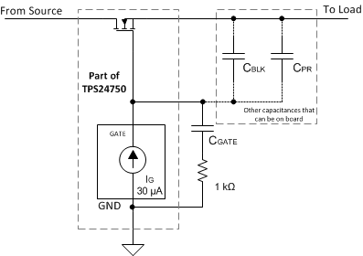
The TPS2475x can be used in applications that expect a constant inrush current. This current is controlled by a capacitor connected from the GATE terminal to GND. A resistor of 1 kΩ placed in series with this capacitor prevents it from slowing a fast-turnoff event. In this mode of operation, the internal FET operates as a source follower, and the slew rate of the output voltage approximately equals the slew rate of the gate voltage (see Figure 43).
To implement a constant-inrush-current circuit, choose the time to charge, ∆t, using Equation 14.

where COUT is the output capacitance, VVCC is the input voltage, and ICHG is the desired charge current. Choose ICHG < PLIM / VVCC to prevent power limiting from affecting the desired current.
To select the gate capacitance use Equation 15. where, IGATE is the nominal gate current and CINTRS, the effective capacitance contributed by the internal FET (approximately 175 pF). In addition, the effect of other capacitances like the capacitance offered by the usage of the Blocking FET (CBLK) and other component capacitances CPR (due to external gate protection diodes, such as Zener diode and board parasitic) to be accounted for arriving at exact value of CGATE. The TIMER capacitor, CT, must be programmed for timing greater than the total turnon time (tON), to ensure and avoid fault detection during start-up.
Typical application circuit with Gate Capacitor (dV/dt) Control Inrush Mode is shown in Figure 43. The turnon waveform with CGATE of 4.7 nF and series resistor of 1 kΩ is shown in Figure 44.

 Figure 43. Gate Capacitor (dV/dt) Control Inrush Mode.