SLVSC87C October 2013 – December 2018 TPS24750 , TPS24751
UNLESS OTHERWISE NOTED, this document contains PRODUCTION DATA.
- 1 Features
- 2 Applications
- 3 Description
- 4 Revision History
- 5 Device Comparison Table
- 6 Pin Configuration and Functions
- 7 Specifications
- 8 Parameter Measurement Information
-
9 Detailed Descriptions
- 9.1 Overview
- 9.2 Functional Block Diagram
- 9.3 Feature Description
- 9.4 Device Functional Modes
-
10Application and Implementation
- 10.1 Application Information
- 10.2
Typical Application
- 10.2.1 Design Requirements
- 10.2.2
Detailed Design Procedure
- 10.2.2.1
Power-Limited Start-Up
- 10.2.2.1.1 STEP 1. Choose RSENSE, RSET, and RIMON
- 10.2.2.1.2 STEP 2. Choose Power-Limit Value, PLIM, and RPROG
- 10.2.2.1.3 STEP 3. Choose Output Voltage Rising Time, tON, and Timing Capacitor CT
- 10.2.2.1.4 STEP 4. Calculate the Retry-Mode Duty Ratio
- 10.2.2.1.5 STEP 5. Select R1, R2, and R3 for UV and OV
- 10.2.2.1.6 STEP 6. Choose R4, R5, and C1
- 10.2.2.2 Alternative Design Example: Gate Capacitor (dv/dt) Control in Inrush Mode
- 10.2.2.3 Additional Design Considerations
- 10.2.2.1
Power-Limited Start-Up
- 10.2.3 Application Curves
- 10.3 System Examples
- 11Power Supply Recommendations
- 12Layout
- 13Device and Documentation Support
- 14Mechanical, Packaging, and Orderable Information
Package Options
Mechanical Data (Package|Pins)
- RUV|36
Thermal pad, mechanical data (Package|Pins)
- RUV|36
Orderable Information
10.2.2.1.3 STEP 3. Choose Output Voltage Rising Time, tON, and Timing Capacitor CT
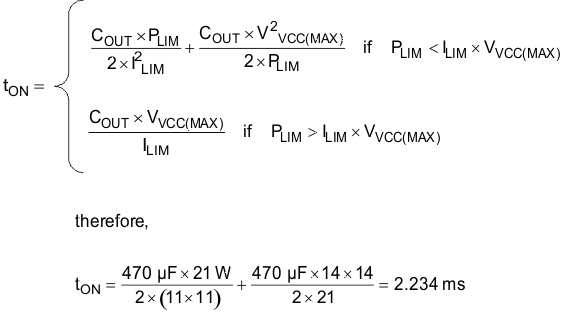
The maximum output voltage rise time, tON, set by timer capacitor CT must suffice to fully charge the load capacitance COUT without triggering the fault circuitry. Equation 9 defines tON for two possible inrush cases. Assuming that only the load capacitance draws current during startup,

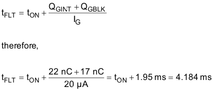
The next step is to determine the minimum fault-timer period. In Equation 9, the output rise time is tON. This is the amount of time it takes to charge the output capacitor up to the final output voltage. However, the fault timer uses the difference between the input voltage and the gate voltage to determine if the TPS2475x is still in inrush limit. The fault timer continues to run until VGS rises 5.8 V (for VVCC = 12 V) above the input voltage. Some additional time must be added to the charge time to account for this additional gate voltage rise. The minimum fault time can be calculated using Equation 10.

where QGINT is the Gate charge of the internal FET to reach the 5.8 V gate voltage (see Figure 25), QGBLK is the Gate charge of blocking FET (for this design, it is considered that CSD17501Q5A SLPS303 blocking FET is used, take this as '0' if blocking FET is not used) and IGATE is the minimum gate sourcing current of the TPS2475x, or 20 μA. Overall, Equation 10 leads to a minimum fault time of 4.184 ms. Considering the tolerances of COUT, CT, ILIM , ITIMER and PLIM, the fault timer must be set to a value ≥ 1.4 times of tFLT obtained, to avoid turning off during start-up, but need to be lower than any maximum fault time limit determined by the device SOA curve (see Figure 27).
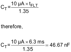
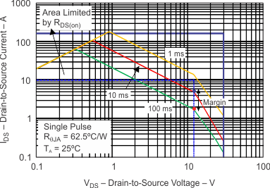
For this example, we select 6.3 ms (1.5 x TFLT) to allow for variation of system parameters such as temperature, load, component tolerance, and input voltage. As per SOA curve (TA = 25oC), for approximately 6.5 ms, the power handled by the device is approximately 70 W at 12 V (value obtained from extrapolation). This need to be scaled (derated) by a factor of (150 –TJDCMAX))/(150 – TA), where TJDCMAX is the maximum steady state junction temperature (TJDMAX = TA(MAX) + ILIM2 × R(DS)ON × RθJA). The scaled power is approximately 34 W. So the power limit of 21 W considered has safe margin of 38% over the derated SOA. This can be depicted through the Figure 42. Also, from Figure 42, from the blue dotted line shown, it can be analyzed that the device at TA = 25oC, can tolerate 12 V and 10 A for approximately time 1 ms and can take power of 21 W for duration of approximately 70 to 75 ms.
The timing capacitor is calculated in Equation 11 as 46.67 nF. Selecting the next-highest standard value, 47 nF, yields a 6.35 ms fault time.

 Figure 42. Design Example SOA