SLVSCU5 March 2015 TPS25200-Q1
PRODUCTION DATA.
- 1 Features
- 2 Applications
- 3 Description
- 4 Simplified Schematic
- 5 Revision History
- 6 Pin Configuration and Functions
- 7 Specifications
- 8 Parameter Measurement Information
- 9 Detailed Description
- 10Application and Implementation
- 11Power Supply Recommendations
- 12Layout
- 13Device and Documentation Support
- 14Mechanical, Packaging, and Orderable Information
Package Options
Mechanical Data (Package|Pins)
- DRV|6
Thermal pad, mechanical data (Package|Pins)
- DRV|6
Orderable Information
10 Application and Implementation
NOTE
Information in the following applications sections is not part of the TI component specification, and TI does not warrant its accuracy or completeness. TI’s customers are responsible for determining suitability of components for their purposes. Customers should validate and test their design implementation to confirm system functionality.
10.1 Application Information
The TPS25200-Q1 device is a 5-V eFuse with precision current-limit and overvoltage clamp. When a slave device such as a mobile data-card device is hot plugged into a USB port as shown in Figure 14, an input transient voltage could damage the slave device because of the cable inductance. Placing the TPS25200-Q1 device at the input of a mobile device as an overvoltage and overcurrent protector can help safeguard the slave device. Input transients also occur when the current through the cable parasitic inductance changes abruptly which can occur when the TPS25200-Q1 device turns off the internal MOSFET in response to an overvoltage or overcurrent event. The TPS25200-Q1 device can withstand the transient without a bypass bulk capacitor, or other external overvoltage protection components at the input side. The TPS25200-Q1 device also can be used at the host side as a traditional power switch that is pin-to-pin compatible with the TPS2553 device.
 Figure 14. Hot Plug into 5-V USB Port With Parasitic Cable Resistance and Inductance
10.2 Typical Application
10.2.1 Overvoltage and Overcurrent Protector
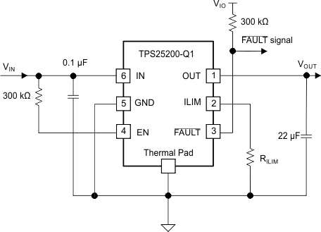 Figure 15. Typical Application Schematic
Use the IOS level listed in the Electrical Characteristics table or the IOS value in the Equation 1 to select the value of RILIM.
10.2.1.1 Design Requirements
For this design example, use the values listed in Table 1 as the input parameters.
Table 1. Design Parameters
| DESIGN PARAMETERS | EXAMPLE VALUE |
|---|---|
| Normal input operation voltage | 5 V |
| Output transient voltage | 6.5 V |
| Minimum current limit | 2.1 A |
| Maximum current limit | 2.9 A |
10.2.1.2 Detailed Design Procedure
10.2.1.2.1 Step by Step Design Produce
To begin the design process a few parameters must be decided upon. The designer needs to know the following:
- Normal Input Operation Voltage
- Output transient voltage
- Minimum Current Limit
- Maximum Current Limit
10.2.1.2.2 Input and Output Capacitance
Input and output capacitance improves the performance of the device; the actual capacitance should be optimized for the particular application. For all applications, a ceramic bypass capacitor with a value of 0.1 µF or greater is recommended between the IN and GND pins. This capacitor should be placed as close to the device as possible for local noise decoupling.
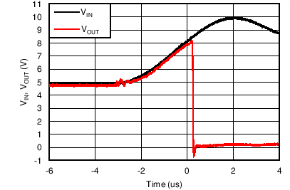
When VIN ramp up exceeds 7.6 V, VOUT follows VIN until the TPS25200-Q1 device turns off the internal MOSFET after t(OVLO_off_delay). Because t(OVLO_off_delay) largely depends on the VIN ramp rate, VOUT receives some peak voltage. Increasing the output capacitance can lower the output peak voltage as shown in Figure 16.
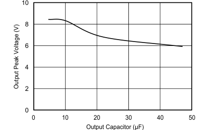 Figure 16. VOUT Peak Voltage vs COUT
(VIN Step From 5 V to 15 V With 1-V/us Ramp-Up Rate)
10.2.1.2.3 Programming the Current-Limit Threshold
The overcurrent threshold is user programmable through an external resistor. The TPS25200-Q1 device uses an internal regulation loop to provide a regulated voltage on the ILIM pin. The current-limit threshold is proportional to the current sourced out of the ILIM pin. The recommended 1% resistor range for RILIM is 36 kΩ ≤ RILIM ≤ 1100 kΩ to ensure stability of the internal regulation loop. Many applications require that the minimum current limit is above a certain current level or that the maximum current limit is below a certain current level. Therefore, considering the tolerance of the overcurrent threshold is important when selecting a value for RILIM. The following equations approximate the resulting overcurrent threshold for a given external resistor value, RILIM. See the Electrical Characteristics table for specific current-limit settings. The traces routing the RILIM resistor to the TPS25200-Q1 device should be as short as possible to reduce parasitic effects on the current-limit accuracy.
RILIM can be selected to provide a current-limit threshold that occurs either above a minimum load current or below a maximum load current.
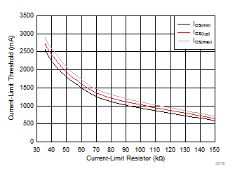
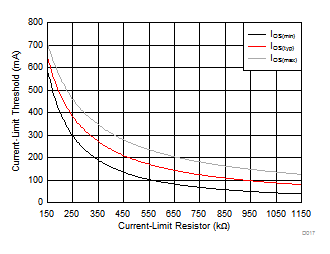
To design above a minimum current-limit threshold, find the intersection of RILIM and the minimum desired load current on the IOS(min) curve. Select a value of RILIM below this value. Programming the current limit above a minimum threshold is important to ensure start up into full load or heavy capacitive loads.
To design below a maximum current-limit threshold, find the intersection of RILIM and the maximum desired load current on the IOS(max) curve. Select a value of RILIM above this value. Programming the current limit below a maximum threshold is important to avoid current limiting the upstream power supplies which causes the input voltage bus to droop.
Use Equation 1, Equation 2, and Equation 3, to calculate the minimum, nominal, and maximum current-limit thresholds for IOS (respectively). For each equation, 36 kΩ ≤ RILIM ≤ 1100 kΩ.


| 36 kΩ ≤ RILIM ≤ 150 KΩ |
| 150 kΩ ≤ RILIM ≤ 1100 KΩ |
10.2.1.2.4 Design Above a Minimum Current Limit
Some applications require that current limiting does not occur below a certain threshold. For this example, assume that 2.1 A must be delivered to the load so that the minimum desired current-limit threshold is 2100 mA. Use Equation 1 and Figure 17 to select a value for RILIM, with IOSmin = 2100 mA, as shown in Equation 4.

Select the closest 1% resistor less than the calculated value: RILIM = 42.2 kΩ. This value sets the minimum current-limit threshold at 2130 mA as shown in Equation 5.

Use Equation 3, Figure 17, and the previously calculated value for RILIM to calculate the maximum resulting current-limit threshold as shown in Equation 6.

The resulting current-limit threshold minimum is 2130 mA and maximum is 2479 mA with RILIM = 42.2kΩ ± 1%.
10.2.1.2.5 Design Below a Maximum Current Limit
Some applications require that current limiting must occur below a certain threshold. For this example, assume that 2.9 A must be delivered to the load so that the minimum desired current-limit threshold is 2900 mA. Use Equation 3 and Figure 18 to select RILIM.

Select the closest 1% resistor greater than the calculated value: RILIM = 36 kΩ. This value sets the maximum current-limit threshold at 2894 mA as shown in Equation 8.

Use Equation 1, Figure 18, and the previously calculated value for RILIM to calculate the minimum resulting current-limit threshold as shown in Equation 9.

The resulting minimum current-limit threshold minimum is 2592 mA and maximum is 2894 mA with RILIM = 36 kΩ ± 1%.
10.2.1.2.6 Power Dissipation and Junction Temperature
The low on-resistance of the internal N-channel MOSFET allows small surface-mount packages to pass large currents. Estimating the power dissipation and junction temperature is good design practice. The following analysis provides an approximation for calculating the junction temperature based on the power dissipation of the package.
NOTE
Thermal analysis is strongly dependent on additional system-level factors. Such factors include air flow, board layout, copper thickness and surface area, and proximity to other devices dissipating power. Good thermal design practice must include all system-level factors in addition to individual component analysis.
Begin by determining the rDS(on) value of the N-channel MOSFET relative to the input voltage (VIN) and operating temperature. As an initial estimate, use the highest operating ambient temperature of interest and read rDS(on) from Figure 4 in the Typical Characteristics section. When VIN is lower than V(OVC), the TPS25200-Q1 device is an traditional power switch. Using this value, calculate the power dissipation with Equation 10.
where
- PD = Total power dissipation (W)
- rDS(on) = Power switch on-resistance (Ω)
- IOUT = Maximum current-limit threshold (A)
When VIN exceeds V(OVC), but is lower than V(OVLO), the TPS25200-Q1 clamp output is fixed to V(OVC). Use Equation 11 to calculate the power dissipation.
where
- V(OVC) = Overvoltage clamp voltage (V)
This step calculates the total power dissipation of the N-channel MOSFET.
Finally, calculate the junction temperature using Equation 12.
where
- RθJA = Thermal resistance (°C/W)
- TA = Ambient temperature (°C)
Compare the calculated junction temperature with the initial estimate. If these two values are not within a few degrees, repeat the calculation using the refined rDS(on) value from the previous calculation as the new estimate. Two or three iterations are generally sufficient to achieve the desired result. The final junction temperature is highly dependent on thermal resistance RθJA, and the thermal resistance is highly dependent on the individual package and board layout.
10.2.1.3 Application Curves
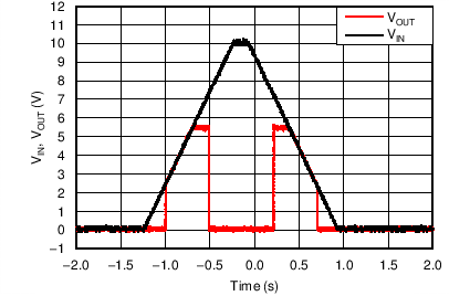
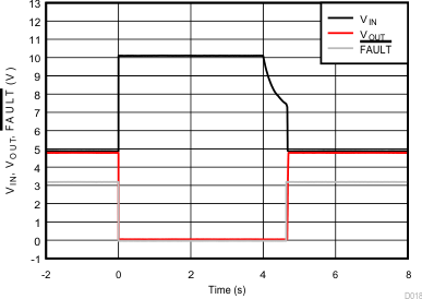
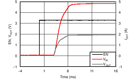
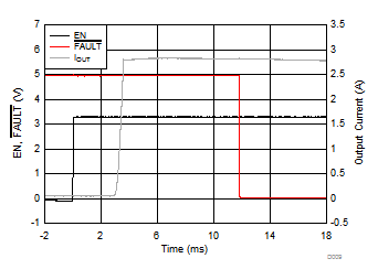
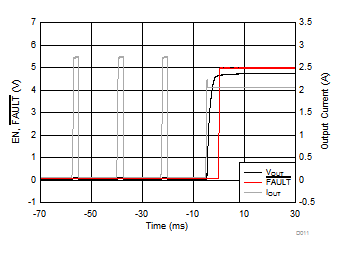
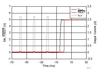
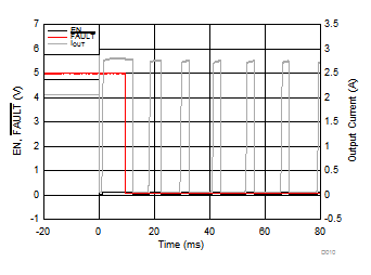
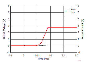
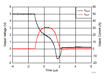 Figure 31. 50-mΩ Hot-Short Response Time
