SLVSFX8A March 2021 – March 2022 TPS2521
PRODUCTION DATA
- 1 Features
- 2 Applications
- 3 Description
- 4 Revision History
- 5 Device Comparison Table
- 6 Pin Configuration and Functions
- 7 Specifications
-
8 Detailed Description
- 8.1 Overview
- 8.2 Functional Block Diagram
- 8.3
Feature Description
- 8.3.1 Input Reverse Polarity Protection
- 8.3.2 Undervoltage Lockout (UVLO and UVP)
- 8.3.3 Overvoltage Clamp (OVC)
- 8.3.4 Inrush Current, Overcurrent, and Short Circuit Protection
- 8.3.5 Analog Load Current Monitor
- 8.3.6 Reverse Current Protection
- 8.3.7 Overtemperature Protection (OTP)
- 8.3.8 Fault Response
- 8.3.9 Power Good Indication (PG)
- 8.4 Device Functional Modes
- 9 Application and Implementation
- 10Power Supply Recommendations
- 11Layout
- 12Device and Documentation Support
- 13Mechanical, Packaging, and Orderable Information
Package Options
Mechanical Data (Package|Pins)
- RPW|10
Thermal pad, mechanical data (Package|Pins)
Orderable Information
9.3.3.4 Setting Power Good Assertion Threshold
The Power Good assertion threshold can be set using the resistors R3 and R4 connected to the PGTH pin whose values can be calculated as:
Equation 12. 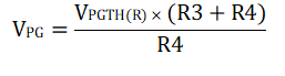
Because R3 and R4 leak the current from the output rail
VOUT, these resistors must be selected to minimize the leakage current.
The current drawn by R3and R4 from the power supply is IR34 = VOUT / (R3 +
R4). However, leakage currents due to external active components connected to the
resistor string can add error to these calculations. So, the resistor string current,
IR34 must be chosen to be 20 times greater than the PGTH leakage current expected. From the device electrical
specifications, PGTH leakage current is 1 μA (maximum), VPGTH(R) = 1.2 V and
from design requirements, VPG = 4.5 V. To solve the equation, first choose
the value of R3 = 100 kΩ and calculate R4 = 36.4 kΩ. Choose nearest 1% standard resistor
value as R4 = 36.5 kΩ.