SLVSFX8A March   2021  – March 2022 TPS2521

PRODUCTION DATA  

  1. Features
  2. Applications
  3. Description
  4. Revision History
  5. Device Comparison Table
  6. Pin Configuration and Functions
  7. Specifications
    1. 7.1 Absolute Maximum Ratings
    2. 7.2 ESD Ratings
    3. 7.3 Recommended Operating Conditions
    4. 7.4 Thermal Information
    5. 7.5 Electrical Characteristics
    6. 7.6 Timing Requirements
    7. 7.7 Switching Characteristics
      1.      15
    8. 7.8 Typical Characteristics
  8. Detailed Description
    1. 8.1 Overview
    2. 8.2 Functional Block Diagram
    3. 8.3 Feature Description
      1. 8.3.1 Input Reverse Polarity Protection
      2. 8.3.2 Undervoltage Lockout (UVLO and UVP)
      3. 8.3.3 Overvoltage Clamp (OVC)
      4. 8.3.4 Inrush Current, Overcurrent, and Short Circuit Protection
        1. 8.3.4.1 Slew Rate (dVdt) and Inrush Current Control
        2. 8.3.4.2 Active Current Limiting
        3. 8.3.4.3 Short-Circuit Protection
      5. 8.3.5 Analog Load Current Monitor
      6. 8.3.6 Reverse Current Protection
      7. 8.3.7 Overtemperature Protection (OTP)
      8. 8.3.8 Fault Response
      9. 8.3.9 Power Good Indication (PG)
    4. 8.4 Device Functional Modes
  9. Application and Implementation
    1. 9.1 Application Information
    2. 9.2 Single Device, Self-Controlled
    3. 9.3 Typical Application
      1. 9.3.1 Application
      2. 9.3.2 Design Requirements
      3. 9.3.3 Detailed Design Procedure
        1. 9.3.3.1 Device Selection
        2. 9.3.3.2 Setting Undervoltage and Overvoltage Thresholds
        3. 9.3.3.3 Setting Output Voltage Rise Time (tR)
        4. 9.3.3.4 Setting Power Good Assertion Threshold
        5. 9.3.3.5 Setting Overcurrent Threshold (ILIM)
        6. 9.3.3.6 Setting Overcurrent Blanking Interval (tITIMER)
      4. 9.3.4 Application Curves
  10. 10Power Supply Recommendations
    1. 10.1 Transient Protection
    2. 10.2 Output Short-Circuit Measurements
  11. 11Layout
    1. 11.1 Layout Guidelines
    2. 11.2 Layout Example
  12. 12Device and Documentation Support
    1. 12.1 Documentation Support
      1. 12.1.1 Related Documentation
    2. 12.2 Receiving Notification of Documentation Updates
    3. 12.3 Support Resources
    4. 12.4 Trademarks
    5. 12.5 Electrostatic Discharge Caution
    6. 12.6 Glossary
  13. 13Mechanical, Packaging, and Orderable Information

Package Options

Mechanical Data (Package|Pins)
Thermal pad, mechanical data (Package|Pins)
Orderable Information

Analog Load Current Monitor

The device allows the system to accurately monitor the output load current by providing an analog current sense output on the ILM pin which is proportional to the current through the FET. The user can sense the voltage (VILM) across the RILM to get a measure of the output load current.

Equation 6. GUID-20210324-CA0I-JJPZ-XG9M-7GRGRBH42VZF-low.gif

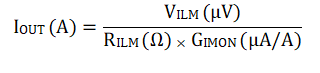
The waveform below shows the ILM signal response to a load step at the output.

GUID-20210327-CA0I-4TSR-8QBS-JWHK8ZLH3DGF-low.gif
VIN = 5 V, COUT = 220 μF, RILM = 750 Ω, IOUT stepped up from 0 A to 4 A
Figure 8-5 Analog Load Current Monitor Response
Note: The ILM pin is sensitive to capacitive loading. Careful design and layout is needed to ensure the parasitic capacitive loading on the ILM pin is < 50 pF for stable operation.