SLUSCE3C October   2015  – August 2020 TPS2549-Q1

PRODUCTION DATA  

  1. Features
  2. Applications
  3. Description
  4. Revision History
  5. Pin Configuration and Functions
  6. Specifications
    1. 6.1 Absolute Maximum Ratings
    2. 6.2 ESD Ratings
    3. 6.3 Recommended Operating Conditions
    4. 6.4 Thermal Information
    5. 6.5 Electrical Characteristics
    6. 6.6 Switching Characteristics
    7. 6.7 Typical Characteristics
  7. Parameter Measurement Information
  8. Detailed Description
    1. 8.1 Overview
    2. 8.2 Functional Block Diagram
    3. 8.3 Feature Description
      1. 8.3.1  FAULT Response
      2. 8.3.2  Cable Compensation
        1. 8.3.2.1 Design Procedure
      3. 8.3.3  D+ and D– Protection
      4. 8.3.4  Output and D+ or D– Discharge
      5. 8.3.5  Port Power Management (PPM)
        1. 8.3.5.1 Benefits of PPM
        2. 8.3.5.2 PPM Details
        3. 8.3.5.3 Implementing PPM in a System With Two Charging Ports (CDP and SDP1)
        4. 8.3.5.4 Implementing PPM in a System With Two Charging Ports (DCP and DCP1)
      6. 8.3.6  CDP and SDP Auto Switch
      7. 8.3.7  Overcurrent Protection
      8. 8.3.8  Undervoltage Lockout
      9. 8.3.9  Thermal Sensing
      10. 8.3.10 Current Limit Setting
    4. 8.4 Device Functional Modes
      1. 8.4.1 Device Truth Table (TT)
      2. 8.4.2 USB Specification Overview
      3. 8.4.3 Standard Downstream Port (SDP) Mode — USB 2.0 and USB 3.0
      4. 8.4.4 Charging Downstream Port (CDP) Mode
      5. 8.4.5 Dedicated Charging Port (DCP) Mode
        1. 8.4.5.1 DCP BC1.2 and YD/T 1591-2009
        2. 8.4.5.2 DCP Divider-Charging Scheme
        3. 8.4.5.3 DCP 1.2-V Charging Scheme
      6. 8.4.6 DCP Auto Mode
      7. 8.4.7 Client Mode
      8. 8.4.8 High-Bandwidth Data-Line Switches
  9. Application and Implementation
    1. 9.1 Application Information
    2. 9.2 Typical Application
      1. 9.2.1 Design Requirements
      2. 9.2.2 Detailed Design Procedure
        1. 9.2.2.1 Input and Output Capacitance
        2. 9.2.2.2 Cable Compensation Calculation
        3. 9.2.2.3 Power Dissipation and Junction Temperature
    3. 9.3 Application Curves
  10. 10Power Supply Recommendations
  11. 11Layout
    1. 11.1 Layout Guidelines
    2. 11.2 Layout Example
  12. 12Device and Documentation Support
    1. 12.1 Documentation Support
      1. 12.1.1 Related Documentation
    2. 12.2 Receiving Notification of Documentation Updates
    3. 12.3 Support Resources
    4. 12.4 Trademarks
    5. 12.5 Electrostatic Discharge Caution
    6. 12.6 Glossary
  13. 13Mechanical, Packaging, and Orderable Information

Package Options

Mechanical Data (Package|Pins)
Thermal pad, mechanical data (Package|Pins)
Orderable Information

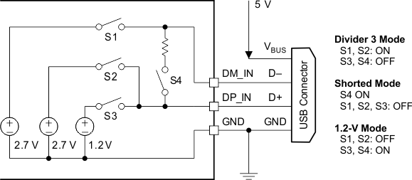
DCP Auto Mode

As previously discussed, the TPS2549-Q1 device integrates an auto-detect state machine that supports all the DCP charging schemes. The auto-detect state machine starts in the Divider3 scheme. However, if a BC1.2 or YD/T 1591-2009 compliant device is attached, the TPS2549-Q1 device responds by turning the power switch back on without output discharge and operating in 1.2-V mode briefly before entering BC1.2 DCP mode. Then the auto-detect state machine stays in that mode until the device releases the data line, in which case the auto-detect state machine goes back to the Divider3 scheme. When a Divider3-compliant device is attached, the TPS2549-Q1 device stays in the Divider3 state.
GUID-26B2BBFD-E5B6-4F84-97A4-53B2567B922B-low.gif Figure 8-11 DCP Auto Mode