SLUSCP2 September   2016 TPS2549

PRODUCTION DATA.  

  1. Features
  2. Applications
  3. Description
  4. Revision History
  5. Pin Configuration and Functions
  6. Specifications
    1. 6.1 Absolute Maximum Ratings
    2. 6.2 ESD Ratings
    3. 6.3 Recommended Operating Conditions
    4. 6.4 Thermal Information
    5. 6.5 Electrical Characteristics
    6. 6.6 Switching Characteristics
    7. 6.7 Typical Characteristics
  7. Parameter Measurement Information
  8. Detailed Description
    1. 8.1 Overview
    2. 8.2 Functional Block Diagram
    3. 8.3 Feature Description
      1. 8.3.1  FAULT Response
      2. 8.3.2  Cable Compensation
        1. 8.3.2.1 Design Procedure
      3. 8.3.3  D+ and D- Protection
      4. 8.3.4  Output and D+ or D- Discharge
      5. 8.3.5  Port Power Management (PPM)
        1. 8.3.5.1 Benefits of PPM
        2. 8.3.5.2 PPM Details
        3. 8.3.5.3 Implementing PPM in a System With Two Charging Ports (CDP and SDP1)
        4. 8.3.5.4 Implementing PPM in a System With Two Charging Ports (DCP and DCP1)
      6. 8.3.6  CDP and SDP Auto Switch
      7. 8.3.7  Overcurrent Protection
      8. 8.3.8  Undervoltage Lockout
      9. 8.3.9  Thermal Sensing
      10. 8.3.10 Current Limit Setting
    4. 8.4 Device Functional Modes
      1. 8.4.1 Device Truth Table (TT)
      2. 8.4.2 USB Specification Overview
      3. 8.4.3 Standard Downstream Port (SDP) Mode — USB 2.0 and USB 3.0
      4. 8.4.4 Charging Downstream Port (CDP) Mode
      5. 8.4.5 Dedicated Charging Port (DCP) Mode
        1. 8.4.5.1 DCP BC1.2 and YD/T 1591-2009
        2. 8.4.5.2 DCP Divider-Charging Scheme
        3. 8.4.5.3 DCP 1.2-V Charging Scheme
      6. 8.4.6 DCP Auto Mode
      7. 8.4.7 Client Mode
      8. 8.4.8 High-Bandwidth Data-Line Switches
  9. Application and Implementation
    1. 9.1 Application Information
    2. 9.2 Typical Application
      1. 9.2.1 Design Requirements
      2. 9.2.2 Detailed Design Procedure
        1. 9.2.2.1 Input and Output Capacitance
        2. 9.2.2.2 Cable Compensation Calculation
        3. 9.2.2.3 Power Dissipation and Junction Temperature
      3. 9.2.3 Application Curves
  10. 10Power Supply Recommendations
  11. 11Layout
    1. 11.1 Layout Guidelines
    2. 11.2 Layout Example
  12. 12Device and Documentation Support
    1. 12.1 Documentation Support
      1. 12.1.1 Related Documentation
    2. 12.2 Receiving Notification of Documentation Updates
    3. 12.3 Community Resources
    4. 12.4 Trademarks
    5. 12.5 Electrostatic Discharge Caution
    6. 12.6 Glossary
  13. 13Mechanical, Packaging, and Orderable Information

Package Options

Mechanical Data (Package|Pins)
Thermal pad, mechanical data (Package|Pins)
Orderable Information

7 Parameter Measurement Information

TPS2549 OUTtestLoad_SLUSCE3.gif Figure 32. OUT Rise-Fall Test Load Figure
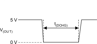
TPS2549 OUTdisch_SLUSCE3.gif Figure 34. OUT Discharge During Mode Change
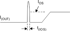
TPS2549 OUTshCkt_SLUSCE3.gif Figure 36. Output Short-Circuit Parameters
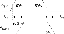
TPS2549 PwrOnOffTim_SLUSCE3.gif Figure 33. Power-On and -Off Timing
TPS2549 EnableTim_SLUSCE3.gif Figure 35. Enable Timing, Active-High Enable