SLUSCO9A September 2016 – October 2016 TPS254900-Q1
PRODUCTION DATA.
- 1 Features
- 2 Applications
- 3 Description
- 4 Revision History
- 5 Pin Configuration and Functions
- 6 Specifications
- 7 Parameter Measurement Information
-
8 Detailed Description
- 8.1 Overview
- 8.2 Functional Block Diagram
- 8.3 Feature Description
- 8.4 Device Functional Modes
- 9 Application and Implementation
- 10Power Supply Recommendations
- 11Layout
- 12Device and Documentation Support
- 13Mechanical, Packaging, and Orderable Information
Package Options
Mechanical Data (Package|Pins)
- RVC|20
Thermal pad, mechanical data (Package|Pins)
Orderable Information
8 Detailed Description
8.1 Overview
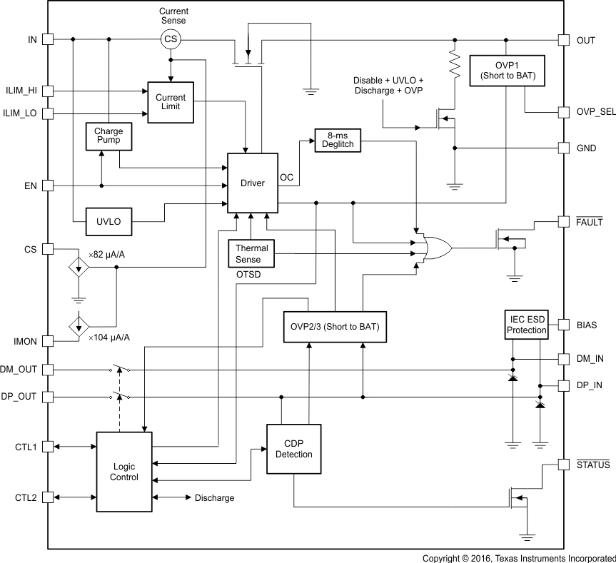
The TPS254900-Q1 device is a USB charging controller and power switch which integrates D+ and D– short-to-battery protection, cable compensation, current monitor (IMON), and IEC ESD protection suitable for automotive USB charging and USB port protection applications.
The integrated power distribution switch uses N-channel MOSFETs suitable for applications where short circuits or heavy capacitive loads will be encountered. The device allows the user to adjust the current-limit thresholds using external resistors. The device enters constant-current mode when the load exceeds the current-limit threshold.
The TPS254900-Q1 device provides VBUS, D+, and D– short-to-battery protection. This protects the upstream voltage regulator, automotive processor, and hub when these pins are exposed to fault conditions.
The device also integrates CDP mode, defined in the BC1.2 specification, to enable up to 1.5-A fast charging of most portable devices during data communication.
The TPS254900-Q1 device integrates a cable compensation (CS) feature to compensate for long-cable voltage drop. This keeps the remote USB port output voltage constant to enhance the user experience under high-current charging conditions.
The TPS254900-Q1 device provides a current-monitor function (IMON) by connecting a resistor from the IMON pin to GND to provide a positive voltage linearly with load current. This can be used for system power or dynamic power management.
Additionally, the device provides ESD protection up to ±8 kV (contact discharge) and ±15 kV (air discharge) per IEC 61000-4-2 on DP_IN and DM_IN.
8.2 Functional Block Diagram
8.3 Feature Description
8.3.1 FAULT Response
The device features an active-low, open-drain fault output. FAULT goes low when there is a fault condition. Fault detection includes overtemperature, overcurrent, or overvoltage on VBUS, DP_IN and DM_IN. Connect a 10-kΩ pullup resistor from FAULT to IN.
Table 1 summarizes the conditions that generate a fault and actions taken by the device.
Table 1. Fault Conditions
| EVENT | CONDITION | ACTION |
|---|---|---|
| Overvoltage on the data lines | V(DP_IN) or V(DM_IN) > 3.9 V | The device immediately shuts off the USB data switches and the internal power switch. The fault indicator asserts with a 16-ms deglitch, and deasserts without deglitch. |
| Overvoltage on V(OUT) | V(OUT) > 6 V or 6.95 V | The device immediately shuts off the internal power switch and the USB data switches. The fault indicator asserts with a 16-ms deglitch and deasserts without deglitch. |
| Overcurrent on V(OUT) | I(OUT) > I(OS) | The device regulates switch current at I(OS) until thermal cycling occurs. The fault indicator asserts and deasserts with an 8-ms deglitch (the device does not assert FAULT on overcurrent in SDP1 mode). |
| Overtemperature | TJ > OTSD2 in non-current-limited or TJ > OTSD1 in current-limited mode. | The device immediately shuts off the internal power switch and the USB data switches. The fault indicator asserts immediately when the junction temperature exceeds OTSD2 or OTSD1 while in a current-limiting condition. The device has a thermal hysteresis of 20°C. |
8.3.2 Cable Compensation
When a load draws current through a long or thin wire, there is an IR drop that reduces the voltage delivered to the load. In the vehicle from the voltage regulator 5-V output to the VPD_IN (input voltage of portable device), the total resistance of power switch rDS(on) and cable resistance causes an IR drop at the PD input. So the charging current of most portable devices is less than their expected maximum charging current.
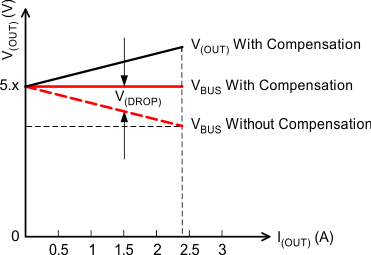 Figure 37. Voltage Drop
TPS254900-Q1 device detects the load current and applies a proportional sink current that can be used to adjust the output voltage of the upstream regulator to compensate for the IR drop in the charging path. The gain G(CS) of the sink current proportional to load current is 82 µA/A.
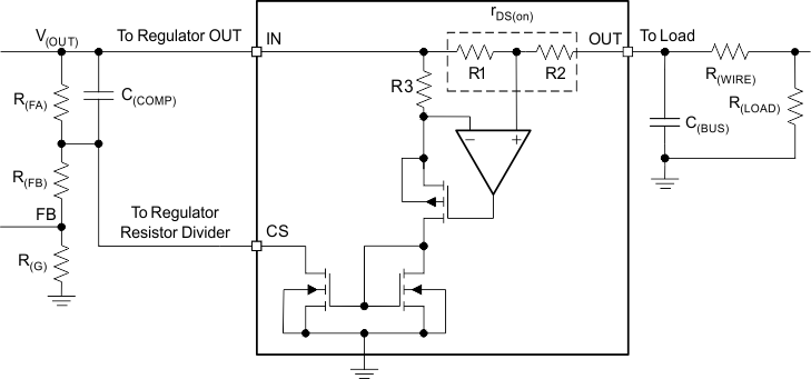 Figure 38. Cable Compensation Equivalent Circuit
8.3.2.1 Design Procedure
To start the procedure, the total resistance, including the power switch rDS(on) and wire resistance R(WIRE), must be known.
- Choose R(G) following the voltage-regulator feedback resistor-divider design guideline.
- Calculate R(FA) according to Equation 1.
- Calculate R(FB) according to Equation 2.
- C(COMP) in parallel with R(FA) is required to stablilize V(OUT) when C(BUS) is large. Start with C(COMP) ≥ 3 × G(CS) × C(OUT), then adjust C(COMP) to optimize the load transient of the voltage regulator output. V(OUT) stability should always be verified in the end application circuit.


8.3.3 D+ and D– Protection
D+ and D– protection consists of ESD and OVP (overvoltage protection). The DP_IN and DM_IN pins provide ESD protection up to ±15 kV (air discharge) and ±8 kV (contact discharge) per IEC 61000-4-2 (see the ESD Ratings section for test conditions).
The ESD stress seen at DP_IN and DM_IN is impacted by many external factors, like the parasitic resistance and inductance between ESD test points and the DP_IN and DM_IN pins. For air discharge, the temperature and humidity of the environment can cause some difference, so the IEC performance should always be verified in the end-application circuit.
The IEC ESD performance of the TPS254900-Q1 device depends on the capacitance connected from BIAS to GND. A 2.2-µF capacitor placed close to the BIAS pin is recommended. Connect the BIAS pin to OUT using a 5.1-kΩ resistor as a discharge path for the ESD stress.
OVP protection is provided for short-to-VBUS or short-to-battery conditions in the vehicle harness, preventing damage to the upstream USB transceiver or hub. When the voltage on DP_IN or DM_IN exceeds 3.9 V (typical), the TPS254900-Q1 device quickly responds to block the high-voltage reverse connection to DP_OUT and DM_OUT. Overcurrent short-to-GND protection for D+ and D– is provided by the upstream USB transceiver.
8.3.4 VBUS OVP Protection
The TPS254900-Q1 OUT pin can withstand up to 18 V. The internal MOSFET turns off quickly when a short-to-battery condition occurs.
The TPS254900-Q1 device has two OVP thresholds; one is 6 V (typical) and the other is 6.95 V (typical). Set the OVP threshold using the external OVP_SEL pin.
8.3.5 Output and D+ or D– Discharge
To allow a charging port to renegotiate current with a portable device, the TPS254900-Q1 device uses the OUT discharge function. During mode change, the TPS254900-Q1 device turns off the power switch while discharging OUT with a 500-Ω resistance, then turning back on the power switches to reassert the OUT voltage.
When an OVP condition occurs on DP_IN or DM_IN, the TPS254900-Q1 device enables an internal 200-kΩ discharge resistance from DP_IN to ground and from DM_IN to ground. The analog switches are also turned off. The TPS254900-Q1 device automatically disables the discharge paths and turns on the analog switches once the OVP condition is removed.
When an OVP condition occurs on OUT, the TPS254900-Q1 device turns on an internal discharge path (see Table 2 for the discharge resistance). The TPS254900-Q1 device automatically turns off the discharge path and turns on the power switch once the OVP condition is removed.
8.3.6 Port Power Management (PPM)
PPM is the intelligent and dynamic allocation of power. PPM is for systems that have multiple charging ports but cannot power them all simultaneously.
8.3.6.1 Benefits of PPM
The benefits of PPM include the following:
- Delivers better user experience
- Prevents overloading of system power supply
- Allows for dynamic power limits based on system state
- Allows every port potentially to be a high-power charging port
- Allows for smaller power-supply capacity because loading is controlled
8.3.6.2 PPM Details
All ports are allowed to broadcast high-current charging. The current limit is based on ILIM_HI. The system monitors the STATUS pin to see when high-current loads are present. Once the allowed number of ports asserts STATUS, the remaining ports are toggled to a non-charging port. The current limit of the non-charging port is based on the ILIM_LO setting. The non-charging ports are automatically toggled back to charging ports when a charging port deasserts STATUS.
STATUS asserts in a charging port when the load current is above ILIM_LO + 30 mA for 210 ms (typical). STATUS deasserts in a charging port when the load current is below ILIM_LO – 20 mA for 3 seconds (typical).
8.3.6.3 Implementing PPM in a System With Two Charging Ports (CDP and SDP1)
Figure 39 shows the implementation of the two charging ports with data communication, each with a TPS254900-Q1 device and configured in CDP mode. In this example, the 5-V power supply for the two charging ports is rated at less than 3.5 A. Both TPS254900-Q1 devices have R(ILIM) chosen to correspond to the low (1-A) and high (2.4-A) current-limit setting for the port. In this implementation, the system can support only one of the two ports at 2.4-A charging current, whereas the other port is set to the SDP1 mode and IOS corresponds to 1 A.
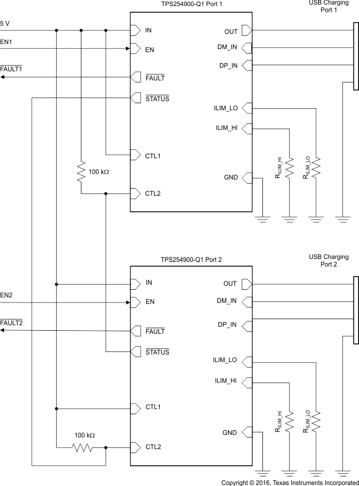 Figure 39. PPM Between CDP and SDP1
8.3.7 Overcurrent Protection
When an overcurrent condition is detected, the device maintains a constant output current and reduces the output voltage accordingly. Two possible overload conditions can occur. In the first condition, the output is shorted before the device is enabled or before the application of V(IN). The TPS254900-Q1 device senses the short and immediately switches into a constant-current output. In the second condition, a short or an overload occurs while the device is enabled. At the instant the overload occurs, high currents flow for 1 to 2 μs (typical) before the current-limit circuit reacts. The device operates in constant-current mode after the current-limit circuit has responded. Complete shutdown occurs only if the fault is present long enough to activate thermal limiting. The device remains off until the junction temperature cools approximately 20°C and then restarts. The device continues to cycle on and off until the overcurrent condition is removed.
8.3.8 Undervoltage Lockout
The undervoltage-lockout (UVLO) circuit disables the power switch until the input voltage reaches the UVLO turnon threshold. Built-in hysteresis prevents unwanted oscillations on the output due to input voltage drop from large current surges.
8.3.9 Thermal Sensing
Two independent thermal-sensing circuits protect the TPS254900-Q1 device if the temperature exceeds recommended operating conditions. These circuits monitor the operating temperature of the power-distribution switch and disable operation. The power dissipation in the package is proportional to the voltage drop across the power switch, so the junction temperature rises during an overcurrent condition. The first thermal sensor turns off the power switch when the die temperature exceeds 135ºC and the device is in current limit. The second thermal sensor turns off the power switch when the die temperature exceeds 155ºC regardless of whether the power switch is in current limit. Hysteresis is built into both thermal sensors, and the switch turns on after the device has cooled by approximately 20°C. The switch continues to cycle off and then on until the fault is removed. The open-drain false-reporting output, FAULT, is asserted (low) during an overtemperature shutdown condition.
8.3.10 Current-Limit Setting
The TPS254900-Q1 has two independent current-limit settings that are each adjusted externally with a resistor. The ILIM_HI setting is adjusted with R(ILIM_HI) connected between ILIM_HI and GND. The ILIM_LO setting is adjusted with R(ILIM_LO) connected between ILIM_LO and GND. Consult the device truth table (Table 3) to see when each current limit is used. Both settings have the same relation between the current limit and the adjusting resistor.
The following equation calculates the value of resistor for adjusting the typical current limit:

Many applications require that the current limit meet specific tolerance limits. When designing to these tolerance limits, both the tolerance of the TPS254900-Q1 current limit and the tolerance of the external adjusting resistor must be taken into account. The following equations approximate the TPS254900-Q1 minimum and maximum current limits to within a few milliamperes and are appropriate for design purposes. The equations do not constitute part of TI’s published device specifications for purposes of TI’s product warranty. These equations assume an ideal—no variation—external adjusting resistor. To take resistor tolerance into account, first determine the minimum and maximum resistor values based on its tolerance specifications and use these values in the equations. Because of the inverse relation between the current limit and the adjusting resistor, use the maximum resistor value in the IOS(min) equation and the minimum resistor value in the IOS(max) equation.


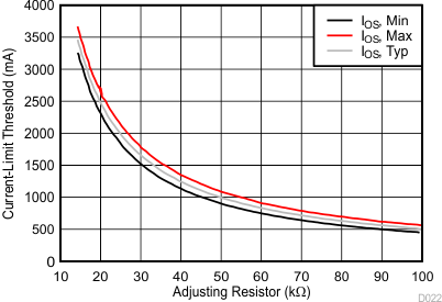
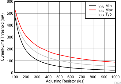
The routing of the traces to the R(ILIM_xx) resistors should have a sufficiently low resistance so as not to affect the current-limit accuracy. The ground connection for the R(ILIM_xx) resistors is also very important. The resistors must reference back to the TPS254900-Q1 GND pin. Follow normal board layout practices to ensure that current flow from other parts of the board does not impact the ground potential between the resistors and the TPS254900-Q1 GND pin.
8.4 Device Functional Modes
8.4.1 Device Truth Table (TT)
The device truth table (Table 3) lists all valid combinations for both control pins (CTL1 and CTL2), and the corresponding charging mode. The TPS254900-Q1 device monitors the CTL inputs and transitions to the charging mode to which it is commanded.
Table 3. Truth Table
| CTL1 | CTL2 | CURRENT LIMIT SELECTED | MODE | STATUS for Load Detect | CS FOR CABLE COMPENSATION | IMON FOR CURRENT MONITOR | FAULT REPORT | NOTES |
|---|---|---|---|---|---|---|---|---|
| 0 | 0 | N/A | Client mode(1) | OFF | OFF | OFF | OFF | Power switch is disabled, only analog switch is on. |
| 0 | 1 | ILIM_LO | SDP | OFF | ON | ON | ON | Standard SDP |
| 1 | 0 | ILIM_LO | SDP1(2) | OFF | ON | ON | ON(3) | No OUT discharge between CDP and SDP1 for PPM |
| 1 | 1 | ILIM_HI | CDP(2) | ON | ON | ON | ON |
8.4.2 USB BC1.2 Specification Overview
The BC1.2 specification includes three different port types:
- Standard downstream port (SDP)
- Charging downstream port (CDP)
- Dedicated charging port (DCP)
BC1.2 defines a charging port as a downstream-facing USB port that provides power for charging portable equipment. Under this definition, CDP and DCP are defined as charging ports.
Table 4 lists the difference between these port types.
Table 4. Operating Modes Table
| PORT TYPE | SUPPORTS USB2.0 COMMUNICATION | MAXIMUM ALLOWABLE CURRENT DRAWN BY PORTABLE EQUIPMENT (A) |
|---|---|---|
| SDP (USB 2.0) | YES | 0.5 |
| SDP (USB 3.0) | YES | 0.9 |
| CDP | YES | 1.5 |
| DCP | NO | 1.5 |
8.4.3 Standard Downstream Port (SDP) Mode — USB 2.0 and USB 3.0
An SDP is a traditional USB port that follows the USB 2.0 or USB 3.0 protocol. An SDP supplies a minimum of 500 mA per port for USB 2.0 and 900 mA per port for USB 3.0. USB 2.0 and USB 3.0 communication is supported, and the host controller must be active to allow charging.
8.4.4 Charging Downstream Port (CDP) Mode
A CDP is a USB port that follows the USB BC1.2 specification and supplies a minimum of 1.5 A per port. A CDP provides power and meets the USB 2.0 requirements for device enumeration. USB 2.0 communication is supported, and the host controller must be active to allow charging. The difference between CDP and SDP is the host-charge handshaking logic that identifies this port as a CDP. A CDP is identifiable by a compliant BC1.2 client device and allows for additional current draw by the client device.
The CDP handshaking process occurs in two steps. During the first step, the portable equipment outputs a nominal 0.6-V output on the D+ line and reads the voltage input on the D– line. The portable device detects the connection to an SDP if the voltage is less than the nominal data-detect voltage of 0.3 V. The portable device detects the connection to a CDP if the D– voltage is greater than the nominal data-detect voltage of 0.3 V and optionally less than 0.8 V.
The second step is necessary for portable equipment to determine whether the equipment is connected to a CDP or a DCP. The portable device outputs a nominal 0.6-V output on the D– line and reads the voltage input on the D+ line. The portable device concludes the equipment is connected to a CDP if the data line being read remains less than the nominal data detects voltage of 0.3 V. The portable device concludes it is connected to a DCP if the data line being read is greater than the nominal data-detect voltage of 0.3 V.
The TPS254900-Q1 integrates CDP detection protocol, used at a downstream port as the CDP controller to support CDP portable-device fast charge up to 1.5 A.
8.4.5 Client Mode
The TPS254900-Q1 device integrates client mode as shown in Figure 42. The internal power switch is OFF to block current flow from OUT to IN, and the signal switches are ON. This mode can be used for software upgrades from the USB port.
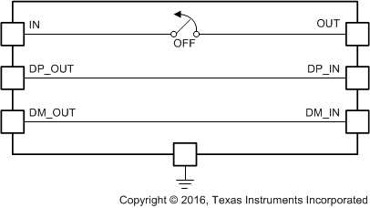 Figure 42. Client-Mode Equivalent Circuit
Passing the IEC 61000-4-2 test for DP_IN and DM_IN requires connecting a discharge resistor to OUT during USB 2.0 high-speed enumeration. In client mode, because the power switch is OFF, OUT must be 5 V so that the device can work normally (usually powered by an external downstream USB port). If the OUT voltage is low, the communication may not work properly.
8.4.6 High-Bandwidth Data-Line Switch
The D+ and D– data lines pass through the device to enable monitoring and handshaking while supporting the charging operation. A wide-bandwidth signal switch allows data to pass through the device without corrupting signal integrity. The data-line switches are turned on in any of the CDP, SDP or client operating modes. The EN input must be at logic high for the data-line switches to be enabled.
NOTE
- While in CDP mode, the data switches are ON, even during CDP handshaking.
- The data switches are only for the USB-2.0 differential pair. In the case of a USB-3.0 host, the super-speed differential pairs must be routed directly to the USB connector without passing through the TPS254900-Q1 device.
- Data switches are OFF during OUT (VBUS) discharge.