SLVSCL5A June 2014 – November 2020 TPS2559
PRODUCTION DATA
- 1 Features
- 2 Applications
- 3 Description
- 4 Revision History
- 5 Device Comparison Table
- 6 Pin Configuration and Functions
- 7 Specifications
- 8 Detailed Description
-
9 Application and Implementation
- 9.1 Application Information
- 9.2
Typical Application
- 9.2.1 Design Requirements
- 9.2.2
Detailed Design Procedure
- 9.2.2.1 Step-by-Step Design Procedure
- 9.2.2.2 Input and Output Capacitance
- 9.2.2.3 Programming the Current-Limit Threshold
- 9.2.2.4 Design Above a Minimum Current Limit
- 9.2.2.5 Design Below a Maximum Current Limit
- 9.2.2.6 Accounting for Resistor Tolerance
- 9.2.2.7 Power Dissipation and Junction Temperature
- 9.2.2.8 Auto-Retry
- 9.2.2.9 Two-Level Current-Limit
- 9.2.3 Application Curves
- 10Power Supply Recommendations
- 11Layout
- 12Device and Documentation Support
- 13Mechanical, Packaging, and Orderable Information
Package Options
Mechanical Data (Package|Pins)
- DRC|10
Thermal pad, mechanical data (Package|Pins)
- DRC|10
Orderable Information
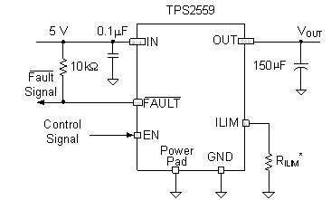
9.2 Typical Application
 Figure 9-1 Typical TPS2559 Power Switch
Use the IOS in the Section 7.5 table or IOS in Equation 1 to select the RILIM.