SLVSCC6A March 2014 – June 2014 TPS2561A-Q1
PRODUCTION DATA.
- 1 Features
- 2 Applications
- 3 Description
- 4 Revision History
- 5 Device Comparison Table
- 6 Pin Functions and Configurations
- 7 Specifications
- 8 Parameter Measurement Information
- 9 Detailed Description
-
10Application and Implementation
- 10.1 Application Information
- 10.2
Typical Application
- 10.2.1
Design Current Limit
- 10.2.1.1 Design Requirements
- 10.2.1.2
Detailed Design Procedure
- 10.2.1.2.1 Determine Design Parameters
- 10.2.1.2.2 Programming the Current-Limit Threshold
- 10.2.1.2.3 Designing Above a Minimum Current Limit
- 10.2.1.2.4 Designing Below a Maximum Current Limit
- 10.2.1.2.5 Accounting for Resistor Tolerance
- 10.2.1.2.6 Power Dissipation and Junction Temperature
- 10.2.1.2.7 Auto-Retry Functionality
- 10.2.1.2.8 Two-Level Current-Limit Circuit
- 10.2.2 Application Curves
- 10.2.1
Design Current Limit
- 11Power Supply Requirements
- 12Layout
- 13Device and Documentation Support
- 14Mechanical, Packaging, and Orderable Information
Package Options
Mechanical Data (Package|Pins)
- DRC|10
Thermal pad, mechanical data (Package|Pins)
- DRC|10
Orderable Information
1 Features
- AEC-Q100 Qualified
- Device HBM ESD Classification Level H2
- Device CDM ESD Classification Level C5
- Two separate current limiting channels
- Meets USB Current-Limiting Requirements
- Adjustable Current Limit, 250 mA–2.8 A (Typ.)
- Accurate 2.1A Min / 2.5A Max Setting
- Fast Short Circuit Response - 3.5-μs (typ)
- Two 44-mΩ High-Side MOSFETs
- Operating Range: 2.5 V to 6.5 V
- 2-μA Maximum Standby Supply Current
- Built-in Soft-Start
- 15 kV / 8 kV System-Level ESD Capable
2 Applications
Automotive USB Charging Ports
3 Description
The TPS2561A-Q1 is dual-channel power-distribution switch intended for automotive applications where precision current limiting is required or heavy capacitive loads and short circuits are encountered. These devices offer a programmable current-limit threshold between 250 mA and 2.8 A (typ) per channel via an external resistor. The power-switch rise and fall times are controlled to minimize current surges during turn on/off.
Each channel of the TPS2561A-Q1 devices limits the output current to a safe level by switching into a constant-current mode when the output load exceeds the current-limit threshold. The FAULTx logic output for each channel independently asserts low during overcurrent and over temperature conditions.
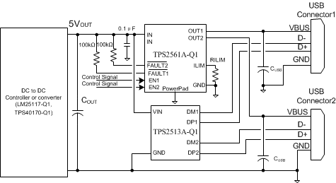
Use with the TPS2511-Q or TPS2513A-Q1 for a low loss, automotive qualified, USB Charging Port Solution capable of charging all of today's popular phones and tablets.
Device Information
| PART NUMBER | PACKAGE | BODY SIZE (NOM) |
|---|---|---|
| TPS2561A-Q1 | SON (10) | 3.00mm x 3.00mm |
Typical Application as Power Switch of Dual Port Automotive USB Charge Port Solution