SLVSE24C November   2017  – August 2019 TPS25820 , TPS25821

PRODUCTION DATA.  

  1. Features
  2. Applications
  3. Description
    1.     Device Images
      1.      Simplified Schematic
  4. Revision History
  5. Pin Configuration and Functions
    1.     Pin Functions
  6. Specifications
    1. 6.1 Absolute Maximum Ratings
    2. 6.2 ESD Ratings
    3. 6.3 Recommended Operating Conditions
    4. 6.4 Thermal Information
    5. 6.5 Electrical Characteristics
    6. 6.6 Switching Characteristics
    7. 6.7 Typical Characteristics
  7. Detailed Description
    1. 7.1 Overview
      1. 7.1.1 USB Type C Basic
      2. 7.1.2 Configuration Channel
      3. 7.1.3 Detecting a Connection
    2. 7.2 Functional Block Diagrams
    3. 7.3 Feature Description
      1. 7.3.1 Configuration Channel Pins CC1 and CC2
      2. 7.3.2 Current Capability Advertisement and VBUS Overload Protection
      3. 7.3.3 FAULT Response
      4. 7.3.4 Thermal Shutdown
      5. 7.3.5 REF
      6. 7.3.6 Plug Polarity Detection
      7. 7.3.7 Sink Attachment Indicator
      8. 7.3.8 Device Enable Control
      9. 7.3.9 Undervoltage Lockout (UVLO)
    4. 7.4 Device Functional Modes
  8. Application and Implementation
    1. 8.1 Application Information
    2. 8.2 Typical Applications
      1. 8.2.1 Type-C Source Port Implementation without BC 1.2 Support
        1. 8.2.1.1 Design Requirements
          1. 8.2.1.1.1 Input and Output Capacitance Considerations
          2. 8.2.1.1.2 System Level ESD Protection
        2. 8.2.1.2 Detailed Design Procedure
        3. 8.2.1.3 Application Curves
      2. 8.2.2 Type -C Source Port Implementation with BC 1.2 (DCP Mode) Support
        1. 8.2.2.1 Design Requirements
        2. 8.2.2.2 Detailed Design Procedure
        3. 8.2.2.3 Application Curves
      3. 8.2.3 Implementing a USB 3.1 Type-C Charging Port with the TPS25820
        1. 8.2.3.1 Design Requirements
        2. 8.2.3.2 Detailed Design Procedure
        3. 8.2.3.3 Application Curves
      4. 8.2.4 Implementing TPS25821 in USB Car Chargers
        1. 8.2.4.1 Design Requirements
        2. 8.2.4.2 Detailed Design Procedure
        3. 8.2.4.3 Application Curves
  9. Power Supply Recommendations
  10. 10Layout
    1. 10.1 Layout Guidelines
    2. 10.2 Layout Example
  11. 11Device and Documentation Support
    1. 11.1 Device Support
      1. 11.1.1 Third-Party Products Disclaimer
    2. 11.2 Documentation Support
      1. 11.2.1 Related Documentation
    3. 11.3 Related Links
    4. 11.4 Receiving Notification of Documentation Updates
    5. 11.5 Community Resources
    6. 11.6 Trademarks
    7. 11.7 Electrostatic Discharge Caution
    8. 11.8 Glossary
  12. 12Mechanical, Packaging, and Orderable Information

Package Options

Mechanical Data (Package|Pins)
Thermal pad, mechanical data (Package|Pins)
Orderable Information

Application Curves

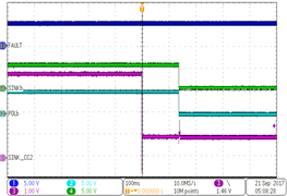
TPS25820 TPS25821 F13_snk_att_slvse24.png
Figure 13. Sink Attach Event
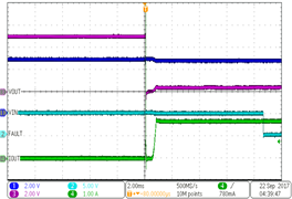
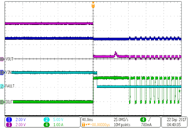
TPS25820 TPS25821 F15_o_shrt_evnt_slvse24.png
COUT = 6.8 µF, Short Output, IN=EN=5V, CC1=Rd, CC2 open
Figure 15. Out Short Event
TPS25820 TPS25821 F17_scrwdrvr_slvse24.png
Figure 17. Screw Driver Short on VBUS
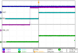
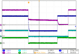
TPS25820 TPS25821 F14_snk_det_slvse24.png
Figure 14. Sink Detach Event
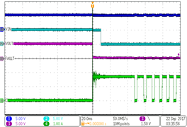
TPS25820 TPS25821 F16_e_o_shrt_evnt_slvse24.png
Figure 16. Extended Period OUT Short Event
TPS25820 TPS25821 F18_brnout_slvse24.png
VIN: 5V ≥ 0V - 5V;1V/ms,365 ms wait,CC1 = Rd,CC2 = open
Figure 18. Brownout Test