SLVSFJ9 September 2021 TPS25854-Q1 , TPS25855-Q1
PRODUCTION DATA
- 1 Features
- 2 Applications
- 3 Description
- 4 Revision History
- 5 Description (Continued)
- 6 Device Comparison Table
- 7 Pin Configuration and Functions
- 8 Specifications
- 9 Parameter Measurement Information
-
10Detailed Description
- 10.1 Overview
- 10.2 Functional Block Diagram
- 10.3
Feature Description
- 10.3.1 Power Down or Undervoltage Lockout
- 10.3.2 Input Overvoltage Protection (OVP) - Continuously Monitored
- 10.3.3 Buck Converter
- 10.3.4 FREQ/SYNC
- 10.3.5 Bootstrap Voltage (BOOT)
- 10.3.6 Minimum ON-time, Minimum OFF-time
- 10.3.7 Internal Compensation
- 10.3.8 Current Limit and Short Circuit Protection
- 10.3.9 Cable Compensation
- 10.3.10 Thermal Management With Temperature Sensing (TS) and OTSD
- 10.3.11 Thermal Shutdown
- 10.3.12 FAULT Indication
- 10.3.13 USB Specification Overview
- 10.3.14 USB Type-C® Basics
- 10.3.15 USB Port Operating Modes
- 10.4 Device Functional Modes
-
11Application and Implementation
- 11.1 Application Information
- 11.2
Typical Applications
- 11.2.1 Design Requirements
- 11.2.2
Detailed Design Procedure
- 11.2.2.1 Output Voltage Setting
- 11.2.2.2 Switching Frequency
- 11.2.2.3 Inductor Selection
- 11.2.2.4 Output Capacitor Selection
- 11.2.2.5 Input Capacitor Selection
- 11.2.2.6 Bootstrap Capacitor Selection
- 11.2.2.7 Undervoltage Lockout Set-Point
- 11.2.2.8 Cable Compensation Set-Point
- 11.2.2.9 FAULT, POL, and THERM_WARN Resistor Selection
- 11.2.3 Application Curves
- 12Power Supply Recommendations
- 13Layout
- 14Device and Documentation Support
- 15Mechanical, Packaging, and Orderable Information
Package Options
Mechanical Data (Package|Pins)
- RPQ|25
Thermal pad, mechanical data (Package|Pins)
Orderable Information
11.2 Typical Applications
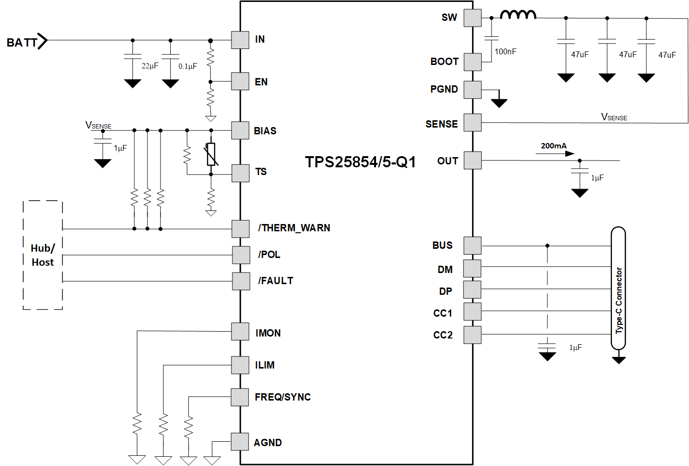
The TPS2585x-Q1 only requires a few external components to convert from a wide voltage range supply to a 5-V output for powering USB devices. Figure 11-1 shows the TPS25855-Q1 typical application schematic for Media HUB.
 Figure 11-1 TPS2585x-Q1 Typical
Application Circuit for 400-KHz fSW
Figure 11-1 TPS2585x-Q1 Typical
Application Circuit for 400-KHz fSWAs a quick start guide, Table 11-1 provides typical component values for some of the most common configurations. The values given in the table are typical. Other values can be used to enhance certain performance criterion as required by the application. The integrated buck regulator of TPS2585x-Q1 is internally compensated and optimized for a reasonable selection of external inductance and capacitance. The external components have to fulfill the needs of the application, but also the stability criteria of the control loop of the device.
| fSW | VOUT Without Cable Compensation | L | CHF + CIN | CBOOT | Rated COUT |
|---|---|---|---|---|---|
| 400 KHZ | 5.1 V | 10 uH | 1 × 100 nF + 1 × 22 uF | 1 × 100 nF | 3 × 47 uF |
| 2.1 MHz | 5.1 V | 2.2 uH | 1 × 100 nF + 1 × 10 uF | 1 × 100 nF | 3 × 22 uF |
- Inductance value is calculated based on max VIN = 18 V.
- All the COUT values are after derating and use low ESR ceramic capacitors.
- The COUT is the buck regulator output capacitors at the SENSE pin.