SLVSFP2B November 2020 – September 2021 TPS25864-Q1 , TPS25865-Q1
PRODUCTION DATA
- 1 Features
- 2 Applications
- 3 Description
- 4 Revision History
- 5 Description (continued)
- 6 Device Comparison Table
- 7 Pin Configuration and Functions
- 8 Specifications
- 9 Parameter Measurement Information
-
10Detailed Description
- 10.1 Overview
- 10.2 Functional Block Diagram
- 10.3
Feature Description
- 10.3.1 Power-Down or Undervoltage Lockout
- 10.3.2 Input Overvoltage Protection (OVP) - Continuously Monitored
- 10.3.3 Buck Converter
- 10.3.4 FREQ/SYNC
- 10.3.5 Bootstrap Voltage (BOOT)
- 10.3.6 Minimum ON-Time, Minimum OFF-Time
- 10.3.7 Internal Compensation
- 10.3.8 Selectable Output Voltage (VSET)
- 10.3.9 Current Limit and Short Circuit Protection
- 10.3.10 Cable Compensation
- 10.3.11 Thermal Management With Temperature Sensing (TS) and OTSD
- 10.3.12 Thermal Shutdown
- 10.3.13 USB Specification Overview
- 10.3.14 USB Port Operating Modes
- 10.4 Device Functional Modes
- 11Application and Implementation
- 12Power Supply Recommendations
- 13Layout
- 14Device and Documentation Support
- 15Mechanical, Packaging, and Orderable Information
Package Options
Mechanical Data (Package|Pins)
- RPQ|25
Thermal pad, mechanical data (Package|Pins)
Orderable Information
8.8 Typical Characteristics
Unless otherwise specified the following conditions apply: VIN = 13.5 V, fSW = 400 kHz, L = 3.3 µH, CSENSE = 141 µF, CPA_BUS = 1 µF, CPB_BUS = 1 µF, TA = 25 °C.
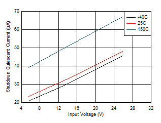
| VEN/EULVO = 0 V | |||
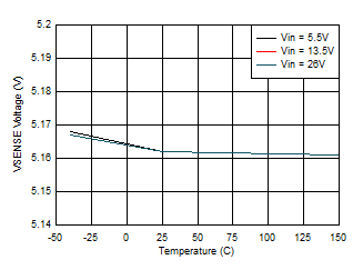
| VSET = GND |
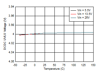
| VEN/EULVO = VSENSE | |||
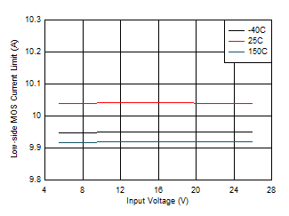 Figure 8-7 Low-side Current Limit vs Input Voltage
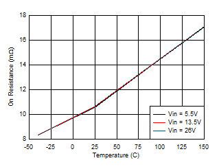
| IPA_BUS = 2.4 A | IPB_BUS = 2.4 A |
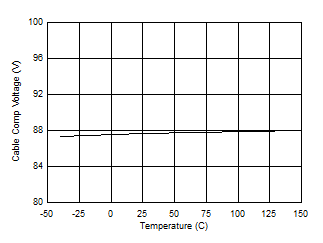
| IPA/B_BUS = 2.4 A | VSET = GND |
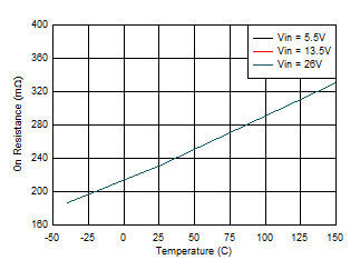 Figure 8-13 OUT
Power Switch On Resistance vs Junction Temperature
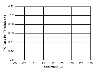 Figure 8-15 TS
Temperature Hot Threshold vs Junction Temperature
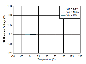 Figure 8-2 Precision Device Enable Threshold
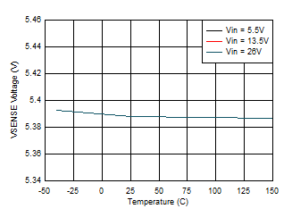
| RVSET = 80.6 kΩ |
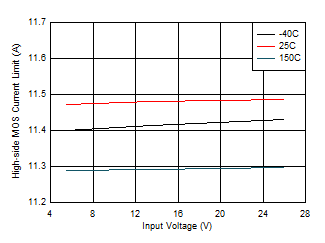 Figure 8-6 High-side Current Limit vs Input Voltage
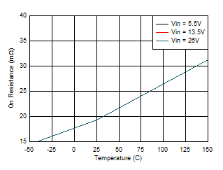
| IPA_BUS = 2.4 A | IPB_BUS = 2.4 A |
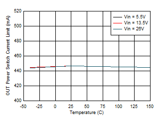 Figure 8-10 OUT
Power Switch Current Limit vs Junction Temperature
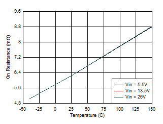 Figure 8-12 USB
Power Switch On Resistance vs Junction Temperature
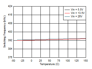
| RFREQ = 49.9 kΩ |
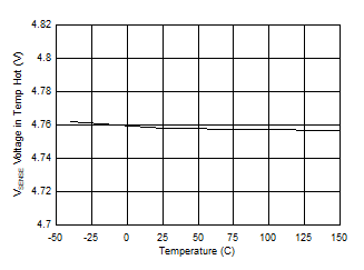 Figure 8-16 SENSE
Voltage in Temperature Hot vs Junction Temperature