SLVSDJ0E May 2016 – January 2021 TPS25940-Q1
PRODMIX
- 1 Features
- 2 Applications
- 3 Description
- 4 Revision History
- 5 Device Comparison Table
- 6 Pin Configuration and Functions
- 7 Specifications
- 8 Parametric Measurement Information
-
9 Detailed Description
- 9.1 Overview
- 9.2 Functional Block Diagram
- 9.3 Feature Description
- 9.4 Device Functional Modes
-
10Application and Implementation
- 10.1 Application Information
- 10.2
Typical Application
- 10.2.1 Design Requirements
- 10.2.2
Detailed Design Procedure
- 10.2.2.1 Step by Step Design Procedure
- 10.2.2.2 Programming the Current-Limit Threshold: R(ILIM) Selection
- 10.2.2.3 Undervoltage Lockout and Overvoltage Set Point
- 10.2.2.4 Programming Current Monitoring Resistor—RIMON
- 10.2.2.5 Setting Output Voltage Ramp Time (tdVdT)
- 10.2.2.6 Programing the Power Good Set Point
- 10.2.2.7 Support Component Selections—R6, R7 and CIN
- 10.2.3 Application Curves
- 10.2.4 System Examples
- 11Power Supply Recommendations
- 12Layout
- 13Device and Documentation Support
- 14Mechanical, Packaging, and Orderable Information
Package Options
Mechanical Data (Package|Pins)
- RVC|20
Thermal pad, mechanical data (Package|Pins)
- RVC|20
Orderable Information
10.2.2.3 Undervoltage Lockout and Overvoltage Set Point
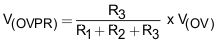
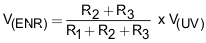
The undervoltage lockout (UVLO) and overvoltage trip point are adjusted using the external voltage divider network of R1, R2 and R3 as connected between IN, EN, OVP and GND pins of the device. The values required for setting the undervoltage and overvoltage are calculated solving Equation 10 and Equation 11.
For minimizing the input current drawn from the power supply {I(R123) = V(IN)/(R1 + R2 + R3)}, it is recommended to use higher values of resistance for R1, R2 and R3.
However, leakage currents because of the external active components connected to the resistor string can add error to these calculations. So, the resistor string current, I(R123) must be chosen to be 20 times greater than the leakage current expected.
From the device electrical specifications, V(OVPR) = 0.99 V and V(ENR) = 0.99 V. For design requirements, V(OV) is 16.5 V and V(UV) is 10.8 V. To solve the equation, first choose the value of R3 = 31.2 kΩ and use Equation 10 to solve for (R1 + R2) = 488.8 kΩ. Use Equation 11 and value of (R1 + R2) to solve for R2 = 16.47 kΩ and finally R1= 472.33 kΩ.
Using the closest standard 1% resistor values gives R1 = 475 kΩ, R2 = 16.7 kΩ, and R3 = 31.2 kΩ.
The power failure threshold is detected on the falling edge of supply. This threshold voltage is 7% lower than the rising threshold, V(UV). This is calculated using Equation 12.