SLVSCE9D June 2014 – October 2017 TPS25942A , TPS25942L , TPS25944A , TPS25944L
UNLESS OTHERWISE NOTED, this document contains PRODUCTION DATA.
- 1 Features
- 2 Applications
- 3 Description
- 4 Revision History
- 5 Device Comparison Table
- 6 Pin Configuration and Functions
- 7 Specifications
- 8 Parameter Measurement Information
-
9 Detailed Description
- 9.1 Overview
- 9.2 Functional Block Diagram
- 9.3
Feature Description
- 9.3.1 Enable and Adjusting Undervoltage Lockout
- 9.3.2 Overvoltage Protection (OVP)
- 9.3.3 Hot Plug-In and In-Rush Current Control
- 9.3.4 Overload and Short Circuit Protection
- 9.3.5 Reverse Current Protection
- 9.3.6 FAULT Response
- 9.3.7 Current Monitoring
- 9.3.8 Power Good Comparator
- 9.3.9 IN, OUT and GND Pins
- 9.3.10 Thermal Shutdown
- 9.4 Device Functional Modes
-
10Application and Implementation
- 10.1 Application Information
- 10.2
Typical Application
- 10.2.1 Design Requirements
- 10.2.2
Detailed Design Procedure
- 10.2.2.1 Step by Step Design Procedure
- 10.2.2.2 Programming the Current-Limit Threshold: R(ILIM) Selection
- 10.2.2.3 Undervoltage Lockout and Overvoltage Set Point
- 10.2.2.4 Programming Current Monitoring Resistor—RIMON
- 10.2.2.5 Setting Output Voltage Ramp Time (tdVdT)
- 10.2.2.6 Programing the Power Good Set Point
- 10.2.2.7 Support Component Selections—R6, R7 and CIN
- 10.2.3 Application Curves
- 10.3 System Examples
- 11Power Supply Recommendations
- 12Layout
- 13Device and Documentation Support
- 14Mechanical, Packaging, and Orderable Information
Package Options
Mechanical Data (Package|Pins)
- RVC|20
Thermal pad, mechanical data (Package|Pins)
- RVC|20
Orderable Information
9.3.1 Enable and Adjusting Undervoltage Lockout
The EN/UVLO pin controls the ON and OFF state of the internal FET. A voltage V(EN/UVLO) < V(ENF) on this pin turns off the internal FET, thus disconnecting IN from OUT, while voltage below 0.6 V takes the device into shutdown mode, with IQ less than 20 µA to ensure minimal power loss. Cycling EN/UVLO low and then back high resets the TPS2594xL that has latched off due to a fault condition.
The internal de-glitch delay on EN/UVLO falling edge is kept low for quick detection of power failure. For applications where a higher de-glitch delay on EN/UVLO is desired, or when the supply is particularly noisy, it is recommended to use an external bypass capacitor from EN/UVLO terminal to GND.
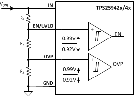
The undervoltage lock out can be programmed by using an external resistor divider from supply IN terminal to EN/UVLO terminal to GND as shown in Figure 50. When an undervoltage or input power fail event is detected, the internal FET is quickly turned off, and FLT is asserted. If the Under-Voltage Lock-Out function is not needed, the EN/UVLO terminal must be connected to the IN terminal. EN/UVLO terminal must not be left floating.
The device also implements internal undervoltage-lockout (UVLO) circuitry on the IN terminal. The device disables when the IN terminal voltage falls below internal UVLO Threshold V(UVF). The internal UVLO threshold has a hysteresis of 115 mV.
 Figure 50. UVLO and OVP Thresholds Set By R1, R2 and R3