SLVSGA8B May 2021 – April 2022 TPS25946
PRODUCTION DATA
- 1 Features
- 2 Applications
- 3 Description
- 4 Revision History
- 5 Device Comparison Table
- 6 Pin Configuration and Functions
- 7 Specifications
-
8 Detailed Description
- 8.1 Overview
- 8.2 Functional Block Diagram
- 8.3
Feature Description
- 8.3.1 Undervoltage Lockout (UVLO and UVP)
- 8.3.2 Overvoltage Lockout (OVLO)
- 8.3.3 Inrush Current, Overcurrent, and Short-Circuit Protection
- 8.3.4 Analog Load Current Monitor
- 8.3.5 Reverse Current Protection
- 8.3.6 Overtemperature Protection (OTP)
- 8.3.7 Fault Response and Indication (FLT)
- 8.3.8 Power Good Indication (PG)
- 8.3.9 Input Supply Good Indication (SPLYGD)
- 8.4 Device Functional Modes
-
9 Application and Implementation
- 9.1 Application Information
- 9.2
Typical Application
- 9.2.1 Design Requirements
- 9.2.2
Detailed Design Procedure
- 9.2.2.1 Device Selection
- 9.2.2.2 Setting Overvoltage Threshold
- 9.2.2.3 Setting Output Voltage Rise Time (tR)
- 9.2.2.4 Setting Power Good Assertion Threshold
- 9.2.2.5 Setting Overcurrent Threshold (ILIM)
- 9.2.2.6 Setting Overcurrent Blanking Interval (tITIMER)
- 9.2.2.7 Selecting External Bias Resistor (R5)
- 9.2.2.8 Selecting External Diode (D1)
- 9.2.3 Application Curve
- 10Power Supply Recommendations
- 11Layout
- 12Device and Documentation Support
- 13Mechanical, Packaging, and Orderable Information
Package Options
Mechanical Data (Package|Pins)
- RPW|10
Thermal pad, mechanical data (Package|Pins)
Orderable Information
9.2.2.7 Selecting External Bias Resistor (R5)
During OTG mode of operation, initially the TPS259460A is in OFF state. The initial bias voltage at the USB bus provided by external diode (D1) and resistor (R5) can be calculated as:

Where
VOUT = Voltage at OUT pin provided by the charger IC in OTG boost mode
VF = diode forward voltage drop
ILOAD = current drawn by USB powered peripheral initially
The bus voltage must be greater than VUVP(R) to ensure the TPS259460A can turn on and start delivering the full load current demanded by the USB peripheral. Putting the value of VF = 0.4 V, VOUT (minimum) = 4.5 V, VUVP(R) = 2.53 V, ILOAD = 100 mA gives maximum value of R5 = 15.7 Ω. Choose value as 11 Ω.
Initial power dissipation across R5 can be calculated as:
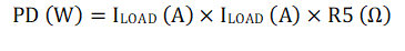
For ILOAD = 100 mA and R5 = 11 Ω, the power dissipation in the resistor is 0.11 W. Choose a resistor with power rating higher than this value for safe operation. A 0.25-W resistor must be suitable for this application.