SLVSFC9B October 2020 – March 2022 TPS25947
PRODUCTION DATA
- 1 Features
- 2 Applications
- 3 Description
- 4 Revision History
- 5 Device Comparison Table
- 6 Pin Configuration and Functions
- 7 Specifications
-
8 Detailed Description
- 8.1 Overview
- 8.2 Functional Block Diagram
- 8.3
Feature Description
- 8.3.1 Input Reverse Polarity Protection
- 8.3.2 Undervoltage Lockout (UVLO and UVP)
- 8.3.3 Overvoltage Lockout (OVLO)
- 8.3.4 Overvoltage Clamp (OVC)
- 8.3.5 Inrush Current, Overcurrent, and Short Circuit Protection
- 8.3.6 Analog Load Current Monitor
- 8.3.7 Reverse Current Protection
- 8.3.8 Overtemperature Protection (OTP)
- 8.3.9 Fault Response and Indication (FLT)
- 8.3.10 Auxiliary Channel Control (AUXOFF)
- 8.3.11 Power Good Indication (PG)
- 8.4 Device Functional Modes
- 9 Application and Implementation
- 10Power Supply Recommendations
- 11Layout
- 12Device and Documentation Support
- 13Mechanical, Packaging, and Orderable Information
Package Options
Mechanical Data (Package|Pins)
- RPW|10
Thermal pad, mechanical data (Package|Pins)
Orderable Information
9.3 Typical Application
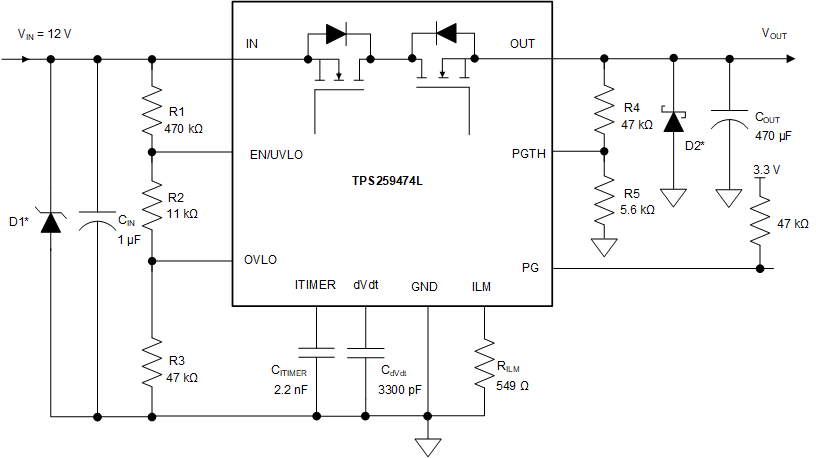
TPS259474x can be used for PCIe card input power protection. A full-sized ×16 graphics card can draw up to 5.5 A at +12 V (66 W). A typical PCIe slot has the capacity of providing current up to 6 A. During overcurrent or short-circuit event at load side, TPS259474x can quickly respond to this fault event by turning off the device and thus protect the load from damage as well as prevent input supply from drooping. The ITIMER feature allows short duration peak currents to pass through without tripping the eFuse, thereby meeting the transient load current profile of graphics cards.

* Optional circuit components needed for transient protection depending on input and output inductance. Please refer to Transient Protection section for details.
Figure 9-2 PCIe Card Input Power Protection