SLVSFC9B October 2020 – March 2022 TPS25947
PRODUCTION DATA
- 1 Features
- 2 Applications
- 3 Description
- 4 Revision History
- 5 Device Comparison Table
- 6 Pin Configuration and Functions
- 7 Specifications
-
8 Detailed Description
- 8.1 Overview
- 8.2 Functional Block Diagram
- 8.3
Feature Description
- 8.3.1 Input Reverse Polarity Protection
- 8.3.2 Undervoltage Lockout (UVLO and UVP)
- 8.3.3 Overvoltage Lockout (OVLO)
- 8.3.4 Overvoltage Clamp (OVC)
- 8.3.5 Inrush Current, Overcurrent, and Short Circuit Protection
- 8.3.6 Analog Load Current Monitor
- 8.3.7 Reverse Current Protection
- 8.3.8 Overtemperature Protection (OTP)
- 8.3.9 Fault Response and Indication (FLT)
- 8.3.10 Auxiliary Channel Control (AUXOFF)
- 8.3.11 Power Good Indication (PG)
- 8.4 Device Functional Modes
- 9 Application and Implementation
- 10Power Supply Recommendations
- 11Layout
- 12Device and Documentation Support
- 13Mechanical, Packaging, and Orderable Information
Package Options
Mechanical Data (Package|Pins)
- RPW|10
Thermal pad, mechanical data (Package|Pins)
Orderable Information
3 Description
The TPS25947xx family of eFuses is a highly integrated circuit protection and power management solution in a small package. The devices provide multiple protection modes using very few external components and are a robust defense against overloads, short-circuits, voltage surges, reverse polarity and excessive inrush current. With integrated back-to-back FETs, reverse current flow from output to input is blocked at all times, making the devices well suited for power MUX/ORing applications as well as systems which need load side energy hold up storage in case input power supply fails. The devices use linear ORing based scheme to ensure almost zero DC reverse current and emulate ideal diode behavior with minimum forward voltage drop and power dissipation.
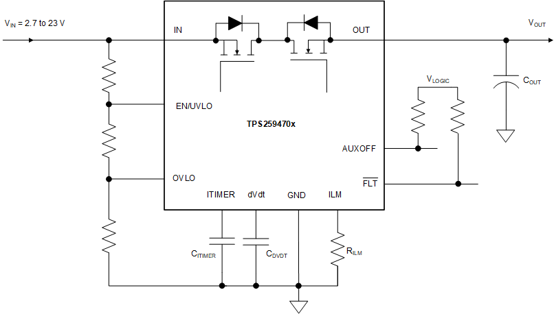
Output slew rate and inrush current can be adjusted using a single external capacitor. Loads are protected from input overvoltage conditions either by clamping the output to a safe fixed maximum voltage (pin selectable), or by cutting off the output if input exceeds an adjustable overvoltage threshold. The devices respond to output overload by actively limiting the current or breaking the circuit. The output current limit threshold as well as the transient overcurrent blanking timer are user adjustable. The current limit control pin also functions as an analog load current monitor.
The devices are available in a 2-mm × 2-mm, 10-pin HotRod QFN package for improved thermal performance and reduced system footprint.
The devices are characterized for operation over a junction temperature range of –40°C to +125°C.
| PART NUMBER | PACKAGE(1) | BODY SIZE (NOM) |
|---|---|---|
| TPS25947xxRPW | QFN (10) | 2 mm × 2 mm |
 Simplified Schematic