SLVSE57C June 2017 – April 2018 TPS2595
PRODUCTION DATA.
- 1 Features
- 2 Applications
- 3 Description
- 4 Revision History
- 5 Device Comparison Table
- 6 Pin Configuration and Functions
- 7 Specifications
-
8 Detailed Description
- 8.1 Overview
- 8.2 Functional Block Diagram
- 8.3 Feature Description
- 8.4 Device Functional Modes
-
9 Application and Implementation
- 9.1 Application Information
- 9.2
Typical Application
- 9.2.1 Design Requirements
- 9.2.2 Detailed Design Procedure
- 9.2.3 Support Component Selection: CIN
- 9.2.4 Application Curves
- 9.2.5 Controlled Power Down (Quick Output Discharge) using TPS2595x5
- 9.2.6 Overvoltage Lockout using TPS259573
- 10Power Supply Recommendations
- 11Layout
- 12Device and Documentation Support
- 13Mechanical, Packaging, and Orderable Information
Package Options
Mechanical Data (Package|Pins)
- DSG|8
Thermal pad, mechanical data (Package|Pins)
- DSG|8
Orderable Information
8.3.1 Undervoltage Protection (UVP) and Undervoltage Lockout (UVLO)
All the TPS2595xx devices constantly monitor the input supply to ensure that the load is powered up only when the voltage is at a sufficient level. During the start-up condition, the device waits for the input supply to rise above a fixed threshold VUVP before it proceeds to turn ON the FET. Similarly, during the ON condition, if the input supply falls below the UVP threshold, the FET is turned OFF. The UVP rising and falling thresholds are slightly different, thereby providing some hysteresis and ensuring stable operation around the threshold voltage.
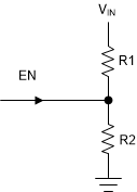
The TPS2595x0, TPS2595x1, TPS2595x5 devices provide an user programmable UVLO mechanism to ensure that the load is powered up only when the voltage is at a sufficient level. This can be achieved by dividing the input supply and feeding it to the EN/UVLO pin. Whenever the voltage at the EN/UVLO pin falls below a threshold VUVLO, the device turns OFF the FET. The FET is turned ON again when the voltage rises above the threshold. The rising and falling thresholds on this pin are slightly different, thereby providing some hysteresis and ensuring stable operation around the threshold voltage.
The user must choose the resistor divider values appropriately to map the desired input undervoltage level to the UVLO threshold of the part. See Figure 47.
 Figure 47. Undervoltage Lockout
