SLVSGG5C november 2021 – april 2023 TPS2597
PRODUCTION DATA
- 1 Features
- 2 Applications
- 3 Description
- 4 Revision History
- 5 Device Comparison Table
- 6 Pin Configuration and Functions
- 7 Specifications
-
8 Detailed Description
- 8.1 Overview
- 8.2 Functional Block Diagram
- 8.3
Feature Description
- 8.3.1 Undervoltage Lockout (UVLO and UVP)
- 8.3.2 Overvoltage Lockout (OVLO)
- 8.3.3 Overvoltage Clamp (OVC)
- 8.3.4 Inrush Current, Overcurrent, and Short Circuit Protection
- 8.3.5 Analog Load Current Monitor
- 8.3.6 Overtemperature Protection (OTP)
- 8.3.7 Fault Response and Indication (FLT)
- 8.3.8 Power-Good Indication (PG)
- 8.4 Device Functional Modes
- 9 Application and Implementation
- 10Device and Documentation Support
- 11Mechanical, Packaging, and Orderable Information
Package Options
Mechanical Data (Package|Pins)
- RPW|10
Thermal pad, mechanical data (Package|Pins)
Orderable Information
3 Description
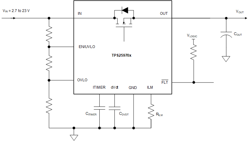
The TPS2597xx family of eFuses is a highly integrated circuit protection and power management solution in a small package. The devices provide multiple protection modes using very few external components and are a robust defense against overloads, short-circuits, voltage surges and excessive inrush current.
Output slew rate and inrush current can be adjusted using a single external capacitor. Loads are protected from input overvoltage conditions either by clamping the output to a safe fixed maximum voltage (pin selectable), or by cutting off the output if the input exceeds an adjustable overvoltage threshold. The devices respond to output overload by actively limiting the current or breaking the circuit. The output current limit threshold as well as the transient overcurrent blanking timer are user adjustable. The current limit control pin also functions as an analog load current monitor.
The devices are available in a 2-mm × 2-mm, 10-pin HotRod™ QFN package for improved thermal performance and reduced system footprint.
The devices are characterized for operation over a junction temperature range of –40°C to +125°C.
| PART NUMBER | PACKAGE(1) | BODY SIZE (NOM) |
|---|---|---|
| TPS2597xxRPW | RPW (QFN, 10) | 2.00 mm × 2.00 mm |
 Simplified Schematic