SLVSEI3C October 2018 – May 2020 TPS25982
PRODUCTION DATA.
- 1 Features
- 2 Applications
- 3 Description
- 4 Revision History
- 5 Device Comparison Table
- 6 Pin Configuration and Functions
- 7 Specifications
-
8 Detailed Description
- 8.1 Overview
- 8.2 Functional Block Diagram
- 8.3 Feature Description
- 8.4 Fault Response
- 8.5 Device Functional Modes
-
9 Application and Implementation
- 9.1 Application Information
- 9.2
Typical Application: Standby Power Rail Protection in Datacenter Servers
- 9.2.1 Design Requirements
- 9.2.2
Detailed Design Procedure
- 9.2.2.1 Device Selection
- 9.2.2.2 Setting the Current Limit Threshold: RILIM Selection
- 9.2.2.3 Setting the Undervoltage Lockout Set Point
- 9.2.2.4 Choosing the Current Monitoring Resistor: RIMON
- 9.2.2.5 Setting the Output Voltage Ramp Time (TdVdt)
- 9.2.2.6 Setting the Load Handshake (LDSTRT) Delay
- 9.2.2.7 Setting the Transient Overcurrent Blanking Interval (tITIMER)
- 9.2.2.8 Setting the Auto-Retry Delay and Number of Retries
- 9.2.3 Application Curves
- 9.3 System Examples
- 10Power Supply Recommendations
- 11Layout
- 12Device and Documentation Support
- 13Mechanical, Packaging, and Orderable Information
Package Options
Mechanical Data (Package|Pins)
- RGE|24
Thermal pad, mechanical data (Package|Pins)
- RGE|24
Orderable Information
7.7 Switching Characteristics
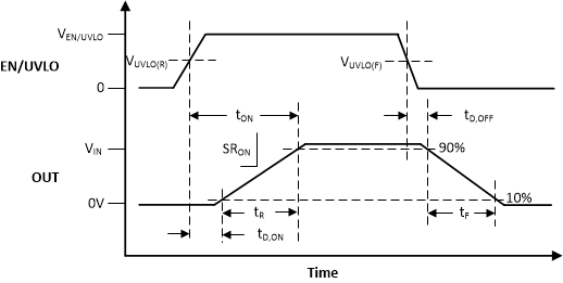
The output rising slew rate is internally controlled and constant across the entire operating voltage range to ensure the turn on timing is not affected by the load conditions. The rising slew rate can be adjusted by adding capacitance from the dVdt pin to ground. As CdVdt is increased it will slow the rising slew rate (SR). See Slew Rate and Inrush Current Control (dVdt) section for more details. The Turn-Off Delay and Fall Time, however, are dependent on the RC time constant of the load capacitance (COUT) and Load Resistance (RL). The Switching Characteristics are only valid for the power-up sequence where the supply is available in steady state condition and the load voltage is completely discharged before the device is enabled.Typical Values are taken at TJ = 25°C unless specifically noted otherwise. RL = 3.6 Ω, COUT = 1 mF| PARAMETER | VIN
|
CdVdt = Open | CdVdt = 3300pF | CdVdt = 6800pF | UNIT | |
|---|---|---|---|---|---|---|
| SRON | Output Rising slew rate | 2.7 V | 6.26 | 1.39 | 0.68 | V/ms |
| 12 V | 7.35 | 1.4 | 0.68 | |||
| 24 V | 7.4 | 1.4 | 0.68 | |||
| tD,ON | Turn on delay | 2.7 V | 1.3 | 1.49 | 1.7 | ms |
| 12 V | 1.24 | 2.1 | 3.01 | |||
| 24 V | 1.2 | 2.91 | 4.74 | |||
| tR | Rise time | 2.7 V | 0.67 | 1.63 | 3.35 | ms |
| 12 V | 1.35 | 6.99 | 14.41 | |||
| 24 V | 2.66 | 13.77 | 28.41 | |||
| tON | Turn on time | 2.7 V | 1.97 | 3.12 | 5.05 | ms |
| 12 V | 2.59 | 9.09 | 17.42 | |||
| 24 V | 3.86 | 16.68 | 33.15 | |||
| tD,OFF | Turn off delay | 2.7 V | 151 | 152 | 152 | µs |
| 12 V | 212 | 212 | 212 | |||
| 24 V | 262 | 262 | 262 | |||
 Figure 1. TPS25982 Switching Times