SLVSEI3C October 2018 – May 2020 TPS25982
PRODUCTION DATA.
- 1 Features
- 2 Applications
- 3 Description
- 4 Revision History
- 5 Device Comparison Table
- 6 Pin Configuration and Functions
- 7 Specifications
-
8 Detailed Description
- 8.1 Overview
- 8.2 Functional Block Diagram
- 8.3 Feature Description
- 8.4 Fault Response
- 8.5 Device Functional Modes
-
9 Application and Implementation
- 9.1 Application Information
- 9.2
Typical Application: Standby Power Rail Protection in Datacenter Servers
- 9.2.1 Design Requirements
- 9.2.2
Detailed Design Procedure
- 9.2.2.1 Device Selection
- 9.2.2.2 Setting the Current Limit Threshold: RILIM Selection
- 9.2.2.3 Setting the Undervoltage Lockout Set Point
- 9.2.2.4 Choosing the Current Monitoring Resistor: RIMON
- 9.2.2.5 Setting the Output Voltage Ramp Time (TdVdt)
- 9.2.2.6 Setting the Load Handshake (LDSTRT) Delay
- 9.2.2.7 Setting the Transient Overcurrent Blanking Interval (tITIMER)
- 9.2.2.8 Setting the Auto-Retry Delay and Number of Retries
- 9.2.3 Application Curves
- 9.3 System Examples
- 10Power Supply Recommendations
- 11Layout
- 12Device and Documentation Support
- 13Mechanical, Packaging, and Orderable Information
Package Options
Mechanical Data (Package|Pins)
- RGE|24
Thermal pad, mechanical data (Package|Pins)
- RGE|24
Orderable Information
8.3.1 Undervoltage Protection (UVLO and UVP)
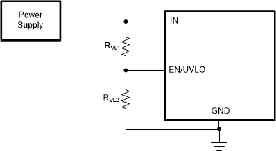
The TPS25982 implements Undervoltage Protection on IN to turn off the output in case the applied voltage becomes too low for the downstream load or the device to operate correctly. The Undervoltage Protection has a default internal threshold of VUVP. If needed, it is also possible to set a user defined Undervoltage Protection threshold higher than VUVP using the UVLO comparator on the EN/UVLO pin. Figure 42 and Equation 1 show how a resistor divider from supply to GND can be used to set the UVLO set point for a given voltage supply level.
 Figure 42. Adjustable Supply UVLO Threshold
The resistors must be sized large enough to minimize the constant leakage from supply to ground through the resistor divider network. At the same time, keep the current through the resistor network sufficiently larger (20x) than the leakage current on the EN/UVLO pin to minimize the error in the resistor divider ratio.