SLVSFQ6A November   2020  – June 2021 TPS2640

PRODUCTION DATA  

  1. Features
  2. Applications
  3. Description
  4. Revision History
  5. Device Comparison
  6. Pin Configuration and Functions
  7. Specifications
    1. 7.1 Absolute Maximum Ratings
    2. 7.2 ESD Ratings
    3. 7.3 Recommended Operating Conditions
    4. 7.4 Thermal Information
    5. 7.5 Electrical Characteristics
    6. 7.6 Timing Requirements
    7. 7.7 Typical Characteristics
  8. Parameter Measurement Information
  9. Detailed Description
    1. 9.1 Overview
    2. 9.2 Functional Block Diagram
    3. 9.3 Feature Description
      1. 9.3.1 Undervoltage Lockout (UVLO)
      2. 9.3.2 Overvoltage Protection (OVP)
      3. 9.3.3 Reverse Input Supply Protection
      4. 9.3.4 Hot Plug-In and In-Rush Current Control
      5. 9.3.5 Overload and Short Circuit Protection
        1. 9.3.5.1 Overload Protection
          1. 9.3.5.1.1 Active Current Limiting
          2. 9.3.5.1.2 Electronic Circuit Breaker with Overload Timeout, MODE = OPEN
        2. 9.3.5.2 Short Circuit Protection
          1. 9.3.5.2.1 Start-Up With Short-Circuit On Output
        3. 9.3.5.3 FAULT Response
          1. 9.3.5.3.1 Look Ahead Overload Current Fault Indicator
        4. 9.3.5.4 Current Monitoring
        5. 9.3.5.5 IN, OUT, RTN, and GND Pins
        6. 9.3.5.6 Thermal Shutdown
        7. 9.3.5.7 Low Current Shutdown Control (SHDN)
    4. 9.4 Device Functional Modes
  10. 10Application and Implementation
    1. 10.1 Application Information
    2. 10.2 Typical Application
      1. 10.2.1 Design Requirements
      2. 10.2.2 Detailed Design Procedure
        1. 10.2.2.1 Step by Step Design Procedure
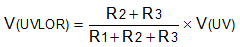
        2. 10.2.2.2 Undervoltage Lockout and Overvoltage Set Point
        3. 10.2.2.3 Programming Current Monitoring Resistor—RIMON
        4. 10.2.2.4 Setting Output Voltage Ramp Time—(tdVdT)
          1. 10.2.2.4.1 Case 1: Start-Up Without Load—Only Output Capacitance C(OUT) Draws Current During Start-Up
          2. 10.2.2.4.2 Case 2: Start-Up With Load—Output Capacitance C(OUT) and Load Draws Current During Start-Up
          3. 10.2.2.4.3 Support Component Selections—RFLTb and C(IN)
      3. 10.2.3 Application Curves
    3. 10.3 System Examples
      1. 10.3.1 Acive ORing Operation
      2. 10.3.2 Field Supply Protection in PLC, DCS I/O Modules
      3. 10.3.3 Simple 24-V Power Supply Path Protection
    4. 10.4 Do's and Dont's
  11. 11Power Supply Recommendations
    1. 11.1 Transient Protection
  12. 12Layout
    1. 12.1 Layout Guidelines
    2. 12.2 Layout Example
  13. 13Device and Documentation Support
    1. 13.1 Device Support
    2. 13.2 Documentation Support
      1. 13.2.1 Related Documentation
    3. 13.3 Receiving Notification of Documentation Updates
    4. 13.4 Support Resources
    5. 13.5 Trademarks
    6. 13.6 Electrostatic Discharge Caution
    7. 13.7 Glossary
  14. 14Mechanical, Packaging, and Orderable Information

Package Options

Mechanical Data (Package|Pins)
Thermal pad, mechanical data (Package|Pins)
Orderable Information

Undervoltage Lockout and Overvoltage Set Point

The undervoltage lockout (UVLO) and overvoltage trip point are adjusted using an external voltage divider network of R1, R2 and R3 connected between IN, UVLO, OVP and RTN pins of the device. The values required for setting the undervoltage and overvoltage are calculated by solving Equation 9 and Equation 10.

Equation 9. GUID-20200603-SS0I-R72M-CQKB-DJCN9DP3VRVN-low.gif
Equation 10. GUID-20200603-SS0I-2KKF-KSQB-N7WFSWQHFCTJ-low.gif

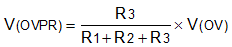
For minimizing the input current drawn from the power supply {I(R123) = V(IN)/(R1+R2+R3)}, it is recommended to use higher value resistance for R1, R2 and R3.

However, the leakage current due to external active components connected at resistor string can add error to these calculations. So, the resistor string current, I(R123) must be chosen to be 20x greater than the leakage current of UVLO and OVP pins.

The UVLO and the OVP pins can also be connected to the RTN pin to enable the internal default V(OV) = 33 V and V(UV) = 15 V.

The power failure is detected on falling edge of the supply. This threshold voltage is 7.5% lower than the rising threshold, V(UV). The voltage at which the device detects power fail can be calculated using Equation 12.

Equation 11. V(PFAIL) 0.925 × V(UV)