SLVSFQ6A November   2020  – June 2021 TPS2640

PRODUCTION DATA  

  1. Features
  2. Applications
  3. Description
  4. Revision History
  5. Device Comparison
  6. Pin Configuration and Functions
  7. Specifications
    1. 7.1 Absolute Maximum Ratings
    2. 7.2 ESD Ratings
    3. 7.3 Recommended Operating Conditions
    4. 7.4 Thermal Information
    5. 7.5 Electrical Characteristics
    6. 7.6 Timing Requirements
    7. 7.7 Typical Characteristics
  8. Parameter Measurement Information
  9. Detailed Description
    1. 9.1 Overview
    2. 9.2 Functional Block Diagram
    3. 9.3 Feature Description
      1. 9.3.1 Undervoltage Lockout (UVLO)
      2. 9.3.2 Overvoltage Protection (OVP)
      3. 9.3.3 Reverse Input Supply Protection
      4. 9.3.4 Hot Plug-In and In-Rush Current Control
      5. 9.3.5 Overload and Short Circuit Protection
        1. 9.3.5.1 Overload Protection
          1. 9.3.5.1.1 Active Current Limiting
          2. 9.3.5.1.2 Electronic Circuit Breaker with Overload Timeout, MODE = OPEN
        2. 9.3.5.2 Short Circuit Protection
          1. 9.3.5.2.1 Start-Up With Short-Circuit On Output
        3. 9.3.5.3 FAULT Response
          1. 9.3.5.3.1 Look Ahead Overload Current Fault Indicator
        4. 9.3.5.4 Current Monitoring
        5. 9.3.5.5 IN, OUT, RTN, and GND Pins
        6. 9.3.5.6 Thermal Shutdown
        7. 9.3.5.7 Low Current Shutdown Control (SHDN)
    4. 9.4 Device Functional Modes
  10. 10Application and Implementation
    1. 10.1 Application Information
    2. 10.2 Typical Application
      1. 10.2.1 Design Requirements
      2. 10.2.2 Detailed Design Procedure
        1. 10.2.2.1 Step by Step Design Procedure
        2. 10.2.2.2 Undervoltage Lockout and Overvoltage Set Point
        3. 10.2.2.3 Programming Current Monitoring Resistor—RIMON
        4. 10.2.2.4 Setting Output Voltage Ramp Time—(tdVdT)
          1. 10.2.2.4.1 Case 1: Start-Up Without Load—Only Output Capacitance C(OUT) Draws Current During Start-Up
          2. 10.2.2.4.2 Case 2: Start-Up With Load—Output Capacitance C(OUT) and Load Draws Current During Start-Up
          3. 10.2.2.4.3 Support Component Selections—RFLTb and C(IN)
      3. 10.2.3 Application Curves
    3. 10.3 System Examples
      1. 10.3.1 Acive ORing Operation
      2. 10.3.2 Field Supply Protection in PLC, DCS I/O Modules
      3. 10.3.3 Simple 24-V Power Supply Path Protection
    4. 10.4 Do's and Dont's
  11. 11Power Supply Recommendations
    1. 11.1 Transient Protection
  12. 12Layout
    1. 12.1 Layout Guidelines
    2. 12.2 Layout Example
  13. 13Device and Documentation Support
    1. 13.1 Device Support
    2. 13.2 Documentation Support
      1. 13.2.1 Related Documentation
    3. 13.3 Receiving Notification of Documentation Updates
    4. 13.4 Support Resources
    5. 13.5 Trademarks
    6. 13.6 Electrostatic Discharge Caution
    7. 13.7 Glossary
  14. 14Mechanical, Packaging, and Orderable Information

Package Options

Mechanical Data (Package|Pins)
Thermal pad, mechanical data (Package|Pins)
Orderable Information
Electronic Circuit Breaker with Overload Timeout, MODE = OPEN

In this mode, during overload events, the device allows the overload current to flow through the device until I(LOAD) < I(FASTRIP). The circuit breaker threshold I(CB) can be programmed using the R(ILIM) resistor as shown in Equation 4.
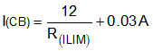
Equation 4. GUID-20200603-SS0I-HPKJ-9JPB-CNZF9KWWDL6X-low.gif

where

  • I(CB) is circuit breaker current threshold in Ampere
  • R(ILIM) is the current limit resistor in kΩ

An internal timer starts when I(CB) < ILOAD < IFASTRIP, and when the timer exceeds tCB(dly), the device turns OFF the internal FET and FLT is asserted. After the internal FET is turned off,

the device commences an auto-retry cycle after 540 ms. The FLT signal remains asserted until the fault condition is removed and the device resumes normal operation. Figure 9-10 and Figure 9-11 illustrate behavior of the system during electronic circuit breaker with auto-retry functionality.

GUID-20200603-SS0I-BSQT-DC9R-XNQ7QWDTV6PQ-low.png

MODE left floating Load Transition from 22 Ω to 12 Ω RILIM = 8 kΩ

Figure 9-10 Circuit Breaker Functionality
GUID-20200603-SS0I-2GT0-MWX9-JH7T805CH8WG-low.png

Load Transition from 22 Ω to 12 Ω , RILIM = 8 kΩ

Figure 9-11 Zoomed at the Instance of Load Step