SLVSFQ6A November 2020 – June 2021 TPS2640
PRODUCTION DATA
- 1 Features
- 2 Applications
- 3 Description
- 4 Revision History
- 5 Device Comparison
- 6 Pin Configuration and Functions
- 7 Specifications
- 8 Parameter Measurement Information
-
9 Detailed Description
- 9.1 Overview
- 9.2 Functional Block Diagram
- 9.3
Feature Description
- 9.3.1 Undervoltage Lockout (UVLO)
- 9.3.2 Overvoltage Protection (OVP)
- 9.3.3 Reverse Input Supply Protection
- 9.3.4 Hot Plug-In and In-Rush Current Control
- 9.3.5 Overload and Short Circuit Protection
- 9.4 Device Functional Modes
-
10Application and Implementation
- 10.1 Application Information
- 10.2 Typical Application
- 10.3 System Examples
- 10.4 Do's and Dont's
- 11Power Supply Recommendations
- 12Layout
- 13Device and Documentation Support
- 14Mechanical, Packaging, and Orderable Information
Package Options
Mechanical Data (Package|Pins)
Thermal pad, mechanical data (Package|Pins)
- PWP|16
Orderable Information
10.3.1 Acive ORing Operation
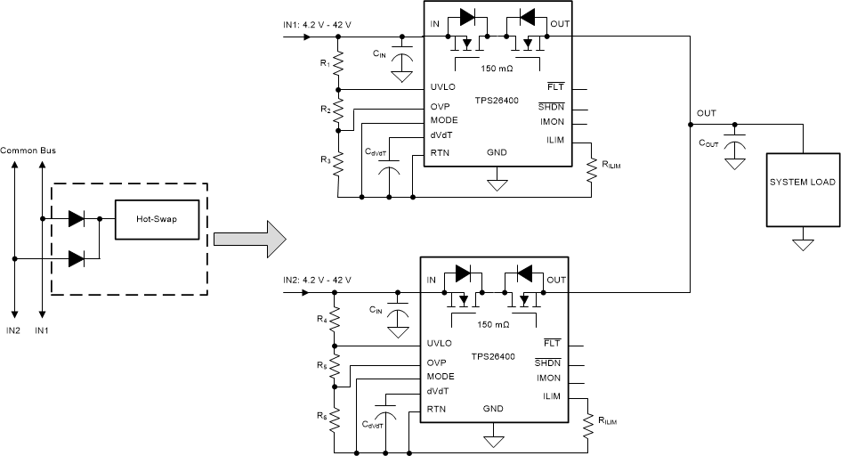
 Figure 10-15 Active ORing Application
Schematic
Figure 10-15 Active ORing Application
SchematicFigure 10-15 shows a typical redundant power supply configuration of the system. Schottky ORing diodes have been popular for connecting parallel power supplies, such as parallel operation of wall adapter with a battery or a hold-up storage capacitor. The disadvantage of using ORing diodes is high voltage drop and associated power loss. The TPS26400 with integrated, N-channel back to back FETs provide a simple and efficient solution.
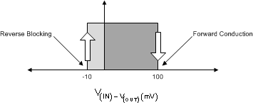
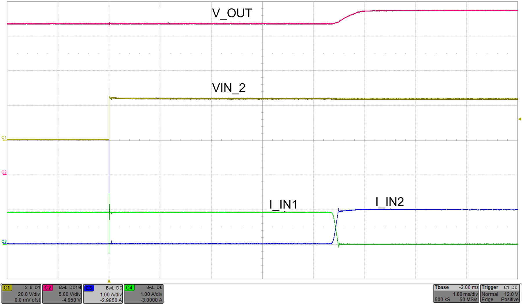
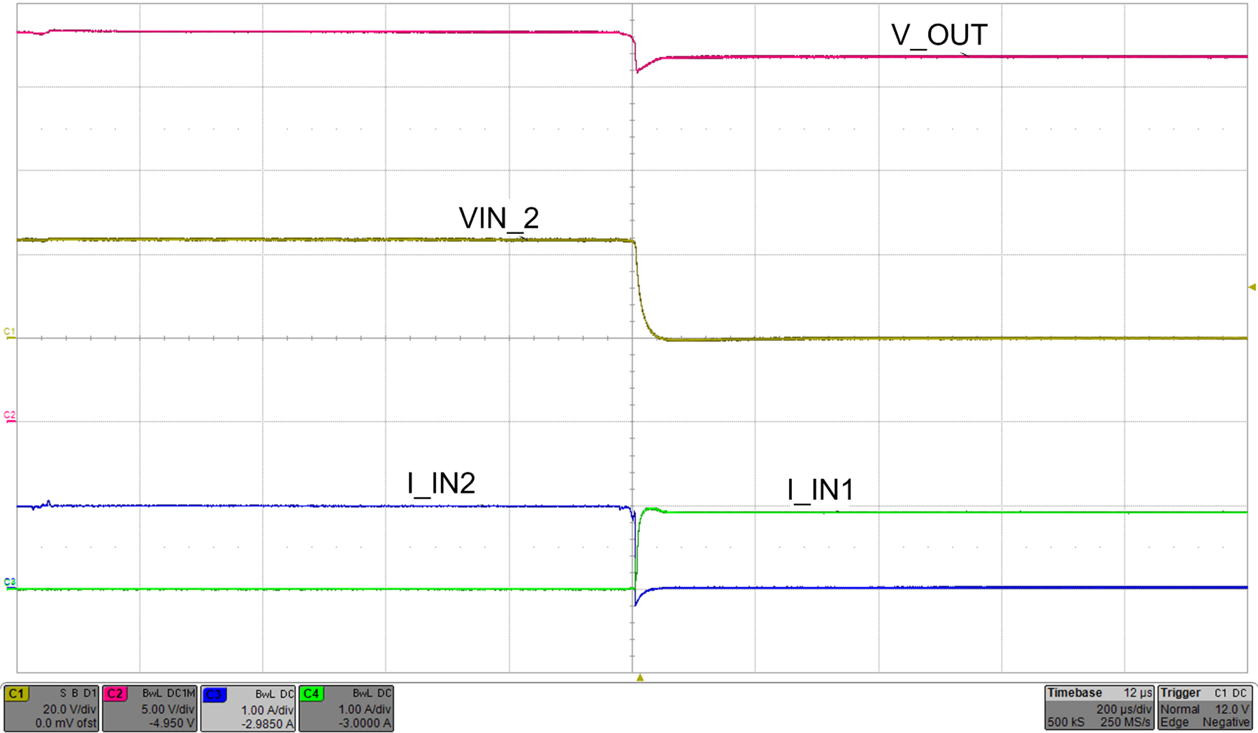
A fast reverse comparator controls the internal FET and it is turned ON or OFF with hysteresis as shown in Figure 10-16. The internal FET is turned off within 1.5 μs (typical) as soon as V(IN) – V(OUT) falls below –110 mV. It turns on within 40 μs (typical) once the differential forward voltage V(IN) – V(OUT) exceeds 100 mV. Figure 10-17 and Figure 10-18 show typical switch-over waveforms of Active ORing implementation using the TPS26400.
 Figure 10-16 Active ORing Thresholds
| VIN1 = 22 V |
Cout = 47 μF VIN2: Plugged In at 24 V |
Rload = 24 Ω C(dVdT) = 22 nF |

| VIN1 = 22 V |
Cout = 47 μF VIN2: Plugged In at 24 V |
Rload = 24 Ω C(dVdT) = 22 nF |
All control pins of the un-powered TPS26400 device in the Active ORing configuration will measure approximately 0.7 V drop with respect to GND. The system micro-controller should ignore IMON and FLT pin voltage measurements of this device when these signals are being monitored.