SLVSFQ6A November   2020  – June 2021 TPS2640

PRODUCTION DATA  

  1. Features
  2. Applications
  3. Description
  4. Revision History
  5. Device Comparison
  6. Pin Configuration and Functions
  7. Specifications
    1. 7.1 Absolute Maximum Ratings
    2. 7.2 ESD Ratings
    3. 7.3 Recommended Operating Conditions
    4. 7.4 Thermal Information
    5. 7.5 Electrical Characteristics
    6. 7.6 Timing Requirements
    7. 7.7 Typical Characteristics
  8. Parameter Measurement Information
  9. Detailed Description
    1. 9.1 Overview
    2. 9.2 Functional Block Diagram
    3. 9.3 Feature Description
      1. 9.3.1 Undervoltage Lockout (UVLO)
      2. 9.3.2 Overvoltage Protection (OVP)
      3. 9.3.3 Reverse Input Supply Protection
      4. 9.3.4 Hot Plug-In and In-Rush Current Control
      5. 9.3.5 Overload and Short Circuit Protection
        1. 9.3.5.1 Overload Protection
          1. 9.3.5.1.1 Active Current Limiting
          2. 9.3.5.1.2 Electronic Circuit Breaker with Overload Timeout, MODE = OPEN
        2. 9.3.5.2 Short Circuit Protection
          1. 9.3.5.2.1 Start-Up With Short-Circuit On Output
        3. 9.3.5.3 FAULT Response
          1. 9.3.5.3.1 Look Ahead Overload Current Fault Indicator
        4. 9.3.5.4 Current Monitoring
        5. 9.3.5.5 IN, OUT, RTN, and GND Pins
        6. 9.3.5.6 Thermal Shutdown
        7. 9.3.5.7 Low Current Shutdown Control (SHDN)
    4. 9.4 Device Functional Modes
  10. 10Application and Implementation
    1. 10.1 Application Information
    2. 10.2 Typical Application
      1. 10.2.1 Design Requirements
      2. 10.2.2 Detailed Design Procedure
        1. 10.2.2.1 Step by Step Design Procedure
        2. 10.2.2.2 Undervoltage Lockout and Overvoltage Set Point
        3. 10.2.2.3 Programming Current Monitoring Resistor—RIMON
        4. 10.2.2.4 Setting Output Voltage Ramp Time—(tdVdT)
          1. 10.2.2.4.1 Case 1: Start-Up Without Load—Only Output Capacitance C(OUT) Draws Current During Start-Up
          2. 10.2.2.4.2 Case 2: Start-Up With Load—Output Capacitance C(OUT) and Load Draws Current During Start-Up
          3. 10.2.2.4.3 Support Component Selections—RFLTb and C(IN)
      3. 10.2.3 Application Curves
    3. 10.3 System Examples
      1. 10.3.1 Acive ORing Operation
      2. 10.3.2 Field Supply Protection in PLC, DCS I/O Modules
      3. 10.3.3 Simple 24-V Power Supply Path Protection
    4. 10.4 Do's and Dont's
  11. 11Power Supply Recommendations
    1. 11.1 Transient Protection
  12. 12Layout
    1. 12.1 Layout Guidelines
    2. 12.2 Layout Example
  13. 13Device and Documentation Support
    1. 13.1 Device Support
    2. 13.2 Documentation Support
      1. 13.2.1 Related Documentation
    3. 13.3 Receiving Notification of Documentation Updates
    4. 13.4 Support Resources
    5. 13.5 Trademarks
    6. 13.6 Electrostatic Discharge Caution
    7. 13.7 Glossary
  14. 14Mechanical, Packaging, and Orderable Information

Package Options

Mechanical Data (Package|Pins)
Thermal pad, mechanical data (Package|Pins)
Orderable Information

Programming Current Monitoring Resistor—RIMON

The voltage at IMON pin V(IMON) represents the voltage proportional to the load current. This can be connected to an ADC of the downstream system for health monitoring of the system. The R(IMON) must be configured based on the maximum input voltage range of the ADC used. R(IMON) is set using Equation 12.

Equation 12. GUID-20200603-SS0I-253X-KLPJ-RNKG9BJXVKKG-low.gif

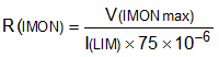
For I(LIM) = 1 A, and considering the operating voltage range of ADC from 0 V to 2.5 V, V(IMONmax) is 2.5 V and R(IMON) is determined by Equation 13.

Equation 13. GUID-20200603-SS0I-DHJK-C47N-KDWFHF4ZV0HK-low.gif

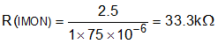
Selecting the R(IMON) value less than determined ensures that ADC limits are not exceeded for maximum value of the load current. Choose the closest standard 1% resistor value: R(IMON) = 33.2 kΩ.

If current monitoring up to I(FASTRIP) is desired, R(IMON) can be reduced by a factor of 1.8 as shown in Equation 5.