SLVSFE3C November 2020 – December 2021 TPS2661
PRODUCTION DATA
- 1 Features
- 2 Applications
- 3 Description
- 4 Revision History
- 5 Device Comparison Table
- 6 Pin Configuration and Functions
- 7 Specifications
-
8 Detailed Description
- 8.1 Overview
- 8.2 Functional Block Diagram
- 8.3
Feature Description
- 8.3.1 Overload Protection and Fast-Trip
- 8.3.2 Reverse Current Blocking for Unipolar Current Inputs TPS26610, TPS26611 and TPS26612 (4–20 mA, 0–20 mA)
- 8.3.3 OUTPUT and INPUT Cutoff During Overvoltage, Undervoltage Due to Miswiring
- 8.3.4 External Power Supply (±Vs)
- 8.3.5 Loop Testing Without ±Vs Supply (Loop Power Mode in TPS26610, TPS26613 Only)
- 8.3.6 Enable Control With TPS26611, TPS26612, and TPS26614
- 8.3.7 Signal Good Indicator (SGOOD)
- 8.4 Device Functional Modes
-
9 Application and Implementation
- 9.1 Application Information
- 9.2 Typical Application: Analog Input Protection for Current Inputs with TPS26610
- 9.3 Typical Application: Analog Input Protection for Multiplexed Current and Voltage Inputs with TPS26611
- 9.4 System Examples
- 10Power Supply Recommendations
- 11Layout
- 12Device and Documentation Support
- 13Mechanical, Packaging, and Orderable Information
Package Options
Mechanical Data (Package|Pins)
- DDF|8
Thermal pad, mechanical data (Package|Pins)
Orderable Information
8.3.1 Overload Protection and Fast-Trip
The TPS2661x devices feature a fixed IOL value of 32-mA typical, bidirectional current limit. For use in unipolar systems like 4–20-mA current loops where negative current is not desired, connect –Vs to GND to cut off when there is a flow of reverse current (OUT to IN). If the current tries to exceed the IOL limit, the device regulates the current, eventually reducing the output voltage. Overload current threshold and time for overload protection can be selected by the MODE pin. See Device Functional Modes for details. The power dissipation across the device during current regulation is (VIN – VOUT) × IOUT, which can heat up the device and lead to thermal shutdown. After thermal shutdown, the device goes into auto retry. The mode pin selects the auto retry period. See Table 8-3 and Figure 8-24 for selection of the auto retry period.
The TPS2661x devices also feature a fast-trip comparator. During fast transient events like output short circuit, miswiring, hotplug, and so forth, the current through the device increases rapidly. Due to limited bandwidth, the current limit amplifier cannot respond quickly to these events . Hence, the fast-trip comparator architecture is included for fast turn OFF of the internal FET during these events. The device turns off the internal FETs within a time of t(FASTTRIP). See the Timing Requirements for t(FASTTRIP). The fast-trip circuit holds the internal FET off for a short duration (50 μs), after which, the device turns back on slowly, allowing the current-limit loop to regulate the output current to current limit as per MODE pin configuration. Figure 8-5 and Figure 8-7 illustrate the current limit behavior of TPS2661x devices. Figure 8-8 illustrates the fast-trip protection of TPS2661x devices and Figure 8-9 illustrates the auto-retry behavior in overload fault.
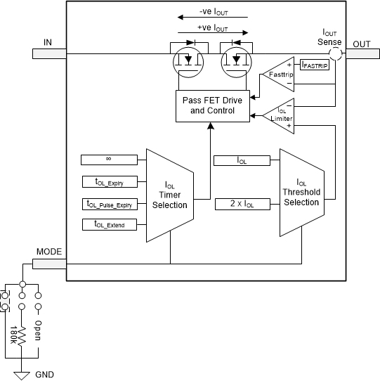 Figure 8-5 Overload Protection and Fast-Trip
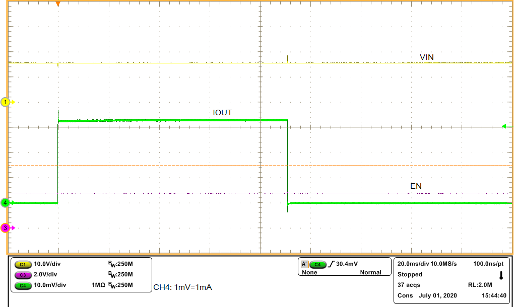 Figure 8-6 Current Limit Behavior for IOUT
< 2 × IOLwith MODE = GND
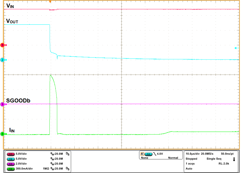 Figure 8-8 Fast-Trip Behavior
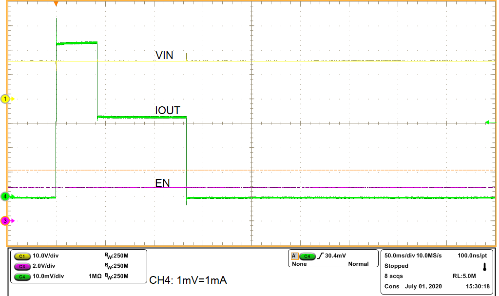 Figure 8-7 Current Limit Behavior for IOUT
> 2 × IOL with MODE = 180 kΩ
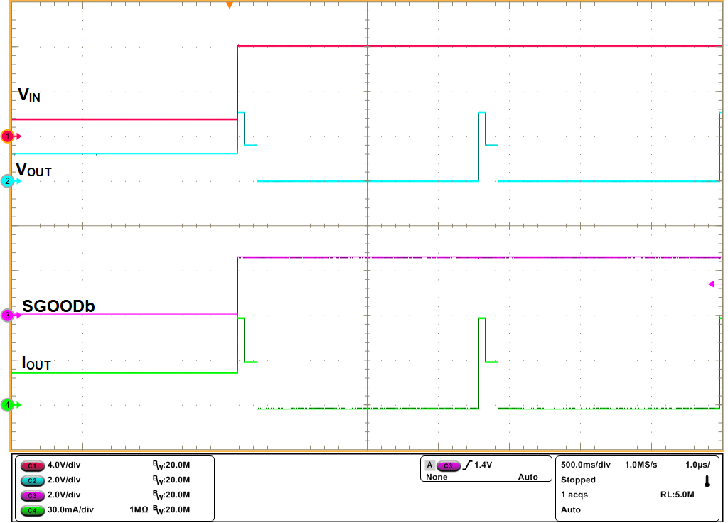 Figure 8-9 Auto-Retry Behavior