SLVSE42B October   2017  – September 2019 TPS27S100

PRODUCTION DATA.  

  1. Features
  2. Applications
  3. Description
    1.     Typical Application Schematic
  4. Revision History
  5. Pin Configuration and Functions
    1.     Pin Functions
  6. Specifications
    1. 6.1 Absolute Maximum Ratings
    2. 6.2 ESD Ratings
    3. 6.3 Recommended Operating Conditions
    4. 6.4 Thermal Information
    5. 6.5 Electrical Characteristics
    6. 6.6 Timing Requirements – Current Monitor Characteristics
    7. 6.7 Switching Characteristics
    8. 6.8 Typical Characteristics
  7. Detailed Description
    1. 7.1 Overview
    2. 7.2 Functional Block Diagram
    3. 7.3 Feature Description
      1. 7.3.1 Accurate Current Monitor
      2. 7.3.2 Adjustable Current Limit
      3. 7.3.3 Inductive-Load Switching-Off Clamp
      4. 7.3.4 Full Protections and Diagnostics
        1. 7.3.4.1 Short-to-GND and Overload Detection
        2. 7.3.4.2 Open-Load Detection
        3. 7.3.4.3 Short-to-Supply Detection
        4. 7.3.4.4 Thermal Fault Detection
        5. 7.3.4.5 UVLO Protection
        6. 7.3.4.6 Loss of GND Protection
        7. 7.3.4.7 Reverse Current Protection
        8. 7.3.4.8 Protection for MCU I/Os
    4. 7.4 Device Functional Modes
      1. 7.4.1 Working Mode
  8. Application and Implementation
    1. 8.1 Application Information
    2. 8.2 Typical Application
      1. 8.2.1 Design Requirements
      2. 8.2.2 Detailed Design Procedure
      3. 8.2.3 Application Curves
  9. Power Supply Recommendations
  10. 10Layout
    1. 10.1 Layout Guidelines
    2. 10.2 Layout Example
      1. 10.2.1 Without a GND Network
      2. 10.2.2 With a GND Network
  11. 11Device and Documentation Support
    1. 11.1 Receiving Notification of Documentation Updates
    2. 11.2 Community Resources
    3. 11.3 Trademarks
    4. 11.4 Electrostatic Discharge Caution
    5. 11.5 Glossary
  12. 12Mechanical, Packaging, and Orderable Information

Package Options

Mechanical Data (Package|Pins)
Thermal pad, mechanical data (Package|Pins)
Orderable Information

Inductive-Load Switching-Off Clamp

When switching an inductive load off, the inductive reactance tends to pull the output voltage negative. Excessive negative voltage could cause the power FET to break down. To protect the power FET, an internal clamp between drain and source is implemented, namely VDS(clamp).
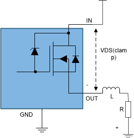
TPS27S100 Image11.gifFigure 27. Drain-to-Source Clamping Structure
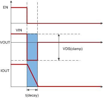
TPS27S100 Image12.gifFigure 28. Inductive-Load Switching-Off Diagram