SBVS344D November   2018  – March 2021 TPS3703-Q1

PRODUCTION DATA  

  1. Features
  2. Applications
  3. Description
  4. Revision History
  5. Device Comparison
  6. Pin Configuration and Functions
  7. Specifications
    1. 7.1 Absolute Maximum Ratings
    2. 7.2 ESD Ratings
    3. 7.3 Recommended Operating Conditions
    4. 7.4 Thermal Information
    5. 7.5 Electrical Characteristics
    6. 7.6 Timing Requirements
    7. 7.7 Timing Diagrams
    8. 7.8 Typical Characteristics
  8. Detailed Description
    1. 8.1 Overview
    2. 8.2 Functional Block Diagram
    3. 8.3 Feature Description
      1. 8.3.1 VDD
      2. 8.3.2 SENSE
      3. 8.3.3 RESET
      4. 8.3.4 Capacitor Time (CT)
      5. 8.3.5 Manual Reset ( MR)
    4. 8.4 Device Functional Modes
      1. 8.4.1 Normal Operation (VDD > VDD(MIN))
      2. 8.4.2 Undervoltage Lockout (VPOR < VDD < UVLO)
      3. 8.4.3 Power-On Reset (VDD < VPOR)
  9. Application and Implementation
    1. 9.1 Application Information
      1. 9.1.1 Voltage Threshold Accuracy
      2. 9.1.2 CT Reset Time Delay
        1. 9.1.2.1 Factory-Programmed Reset Delay Timing
        2. 9.1.2.2 Programmable Reset Delay-Timing
      3. 9.1.3 RESET Latch Mode
      4. 9.1.4 Adjustable Voltage Thresholds
      5. 9.1.5 Immunity to SENSE Pin Voltage Transients
        1. 9.1.5.1 Hysteresis
    2. 9.2 Typical Applications
      1. 9.2.1 Design 1: Multi-Rail Window Monitoring for Microcontroller Power Rails
        1. 9.2.1.1 Design Requirements
        2. 9.2.1.2 Detailed Design Procedure
        3. 9.2.1.3 Application Curves
      2. 9.2.2 Design 2: RESET Latch Mode
        1. 9.2.2.1 Design Requirements
        2. 9.2.2.2 Detailed Design Procedure
        3. 9.2.2.3 Application Curves
  10. 10Power Supply Recommendations
    1. 10.1 Power Supply Guidelines
  11. 11Layout
    1. 11.1 Layout Guidelines
    2. 11.2 Layout Example
  12. 12Device and Documentation Support
    1. 12.1 Device Support
      1. 12.1.1 Device Nomenclature
    2. 12.2 Documentation Support
      1. 12.2.1 Evaluation Module
    3. 12.3 Receiving Notification of Documentation Updates
    4. 12.4 Support Resources
    5. 12.5 Trademarks
    6. 12.6 Electrostatic Discharge Caution
    7. 12.7 Glossary
  13. 13Mechanical, Packaging, and Orderable Information

Package Options

Mechanical Data (Package|Pins)
Thermal pad, mechanical data (Package|Pins)
Orderable Information

CT Reset Time Delay

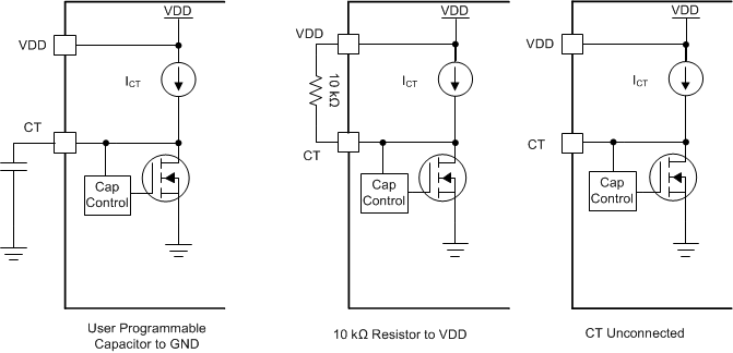
The TPS3703-Q1 features three options for setting the reset delay (tD): connecting a capacitor to the CT pin, connecting a pull-up resistor to VDD, and leaving the CT pin unconnected. Figure 9-2 shows a schematic drawing of all three options. To determine which option is connected to the CT pin, an internal state machine controls the internal pulldown device and measures the pin voltage. This sequence of events takes 450 μs to determine which timing option is used. Every time the voltage on the SENSE line enters the valid window (VIT-(UV) + VHYS < VSENSE < VIT+(OV) -VHYS, the state machine determines the CT option.
GUID-C9882C79-A28E-4121-AEE9-AF4FF55389AC-low.gifFigure 9-2 CT Charging Circuit