SBVS344D November 2018 – March 2021 TPS3703-Q1
PRODUCTION DATA
- 1 Features
- 2 Applications
- 3 Description
- 4 Revision History
- 5 Device Comparison
- 6 Pin Configuration and Functions
- 7 Specifications
- 8 Detailed Description
- 9 Application and Implementation
- 10Power Supply Recommendations
- 11Layout
- 12Device and Documentation Support
- 13Mechanical, Packaging, and Orderable Information
Package Options
Mechanical Data (Package|Pins)
- DSE|6
Thermal pad, mechanical data (Package|Pins)
Orderable Information
9.1.1 Voltage Threshold Accuracy
Voltage monitoring requirements vary depending on the voltage supply tolerance of the device being powered. Due to the high precision of the TPS3703-Q1 (±0.7% Max), the device allows for a wider supply voltage margins and threshold headroom for tight tolerance applications.
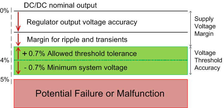
For example, take a DC/DC regulator providing power to a core voltage rail of an MCU. The MCU has a tolerance of ±5% of the nominal output voltage of the DC/DC. The user sets an ideal voltage threshold of ±4% which allows for ±1% of threshold accuracy. Since the TPS3703-Q1 threshold accuracy is higher than ±1%, the user has more supply voltage margin which can allow for a relaxed power supply design. This gives flexibility to the DC/DC to use a smaller output capacitor or inductor because of a larger voltage window for voltage ripple and transients. There is also headroom between the minimum system voltage and voltage tolerance of the MCU to ensure that the voltage supply will never be in the region of potential failure of malfunction without the TPS3703-Q1 asserting a reset signal.
Figure 9-1 illustrates the supply undervoltage margin and accuracy of the TPS3703-Q1 for the example explained above. Using a low accuracy supervisor will eat into the available budget for the power supply ripple and transient response. This gives less flexibility to the user and a more stringent DC/DC converter design.
 Figure 9-1 TPS3703-Q1 Voltage Threshold Accuracy