SGLS143D December   2002  – July 2019 TPS3820-Q1 , TPS3823-Q1 , TPS3824-Q1 , TPS3825-Q1 , TPS3828-Q1

PRODUCTION DATA.  

  1. Features
  2. Applications
  3. Description
    1.     Device Images
      1.      Typical Application Schematic
      2.      Normalized Input Threshold Voltage vs Free-Air Temperature
  4. Revision History
  5. Device Comparison Table
  6. Pin Configuration and Functions
    1.     Pin Functions
  7. Specifications
    1. 7.1 Absolute Maximum Ratings
    2. 7.2 ESD Ratings
    3. 7.3 Recommended Operating Conditions
    4. 7.4 Thermal Information
    5. 7.5 Electrical Characteristics
    6. 7.6 Timing Requirements
    7. 7.7 Switching Characteristics
    8. 7.8 Typical Characteristics
  8. Detailed Description
    1. 8.1 Overview
    2. 8.2 Functional Block Diagram
    3. 8.3 Feature Description
      1. 8.3.1 Manual Reset (MR)
      2. 8.3.2 Active High or Active Low Output
      3. 8.3.3 Push-Pull or Open-Drain Output
      4. 8.3.4 Watchdog Timer (WDI)
    4. 8.4 Device Functional Modes
  9. Application and Implementation
    1. 9.1 Application Information
    2. 9.2 Typical Applications
      1. 9.2.1 Supply Rail Monitoring with Watchdog Time-out and 200-ms Delay
        1. 9.2.1.1 Design Requirements
        2. 9.2.1.2 Detailed Design Procedure
        3. 9.2.1.3 Application Curve
      2. 9.2.2 Decoupling WDI During Reset Event
  10. 10Power Supply Recommendations
  11. 11Layout
    1. 11.1 Layout Guidelines
    2. 11.2 Layout Example
  12. 12Device and Documentation Support
    1. 12.1 Documentation Support
      1. 12.1.1 Related Documentation
        1. 12.1.1.1 Related Links
    2. 12.2 Receiving Notification of Documentation Updates
    3. 12.3 Community Resources
    4. 12.4 Trademarks
    5. 12.5 Electrostatic Discharge Caution
    6. 12.6 Glossary
  13. 13Mechanical, Packaging, and Orderable Information

Package Options

Refer to the PDF data sheet for device specific package drawings

Mechanical Data (Package|Pins)
  • DBV|5
Thermal pad, mechanical data (Package|Pins)
Orderable Information

Decoupling WDI During Reset Event

If the application requires that the input to WDI is active when the reset signal is asserted, Figure 11 shows how to decouple WDI from the active signal using an N-channel FET. The N-channel FET is placed in series with the WDI pin, with the gate of the FET connected to the RESET output.
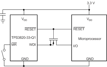
TPS3820-Q1 TPS3823-Q1 TPS3824-Q1 TPS3825-Q1 TPS3828-Q1 wdi_sgls143.gifFigure 11. WDI Example