SBVS301B October   2016  – September 2021 TPS3850

PRODUCTION DATA  

  1. Features
  2. Applications
  3. Description
  4. Revision History
  5. Pin Configuration and Functions
  6. Specifications
    1. 6.1 Absolute Maximum Ratings
    2. 6.2 ESD Ratings
    3. 6.3 Recommended Operating Conditions
    4. 6.4 Thermal Information
    5. 6.5 Electrical Characteristics
    6. 6.6 Timing Requirements
    7. 6.7 Timing Diagrams
    8. 6.8 Typical Characteristics
  7. Detailed Description
    1. 7.1 Overview
    2. 7.2 Functional Block Diagrams
    3. 7.3 Feature Description
      1. 7.3.1 CRST
      2. 7.3.2 RESET
      3. 7.3.3 Over- and Undervoltage Fault Detection
      4. 7.3.4 Adjustable Operation Using the TPS3850H01
      5. 7.3.5 Window Watchdog
        1. 7.3.5.1 SET0 and SET1
          1. 7.3.5.1.1 Enabling the Window Watchdog
          2. 7.3.5.1.2 Disabling the Watchdog Timer When Using the CRST Capacitor
          3. 7.3.5.1.3 SET0 and SET1 During Normal Watchdog Operation
      6. 7.3.6 Window Watchdog Timer
        1. 7.3.6.1 CWD
        2. 7.3.6.2 WDI Functionality
        3. 7.3.6.3 WDO Functionality
    4. 7.4 Device Functional Modes
      1. 7.4.1 VDD is Below VPOR ( VDD < VPOR)
      2. 7.4.2 Above Power-On-Reset But Less Than UVLO (VPOR ≤ VDD < VUVLO)
      3. 7.4.3 Above UVLO But Less Than VDD (min) (VUVLO ≤ VDD < VDD (min))
      4. 7.4.4 Normal Operation (VDD ≥ VDD (min))
  8. Application and Implementation
    1. 8.1 Application Information
      1. 8.1.1 CRST Delay
        1. 8.1.1.1 Factory-Programmed Reset Delay Timing
        2. 8.1.1.2 Programmable Reset Delay-Timing
      2. 8.1.2 CWD Functionality
        1. 8.1.2.1 Factory-Programmed Timing Options
        2. 8.1.2.2 Adjustable Capacitor Timing
      3. 8.1.3 Adjustable SENSE Configuration
      4. 8.1.4 Overdrive on the SENSE Pin
    2. 8.2 Typical Applications
      1. 8.2.1 Design 1: Monitoring a 1.2-V Rail with Factory-Programmable Watchdog Timing
        1. 8.2.1.1 Design Requirements
        2. 8.2.1.2 Detailed Design Procedure
          1. 8.2.1.2.1 Monitoring the 1.2-V Rail
          2. 8.2.1.2.2 Meeting the Minimum Reset Delay
          3. 8.2.1.2.3 Setting the Watchdog Window
          4. 8.2.1.2.4 Calculating the RESET and WDO Pullup Resistor
        3. 8.2.1.3 Application Curves
      2. 8.2.2 Design 2: Using TPS3850H01 to monitor a 0.7-V Rail With an Adjustable Window Watchdog Timing
        1. 8.2.2.1 Design Requirements
        2. 8.2.2.2 Detailed Design Procedure
          1. 8.2.2.2.1 Meeting the Minimum Reset Delay
          2. 8.2.2.2.2 Setting the Window Watchdog
          3. 8.2.2.2.3 Watchdog Disabled During the Initialization Period
          4. 8.2.2.2.4 Calculating the Sense Resistor
        3. 8.2.2.3 Application Curves
  9. Power Supply Recommendations
  10. 10Layout
    1. 10.1 Layout Guidelines
    2. 10.2 Layout Example
  11. 11Device and Documentation Support
    1. 11.1 Device Support
      1. 11.1.1 Device Nomenclature
    2. 11.2 Documentation Support
      1. 11.2.1 Related Documentation
    3. 11.3 Receiving Notification of Documentation Updates
    4. 11.4 Support Resources
    5. 11.5 Trademarks
    6. 11.6 Electrostatic Discharge Caution
    7. 11.7 Glossary
  12. 12Mechanical, Packaging, and Orderable Information

Package Options

Mechanical Data (Package|Pins)
Thermal pad, mechanical data (Package|Pins)
Orderable Information

Adjustable SENSE Configuration

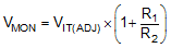
The TPS3850H01 has an undervoltage supervisor that can monitor voltage rails greater than 0.4 V. Table 8-6 contains 1% resistor values for creating a voltage divider to monitor common rails from 0.5 V to 12 V with a threshold of 4% and 10%. These resistor values can be scaled to decrease the amount of current flowing through the resistor divider, but increasing the resistor values also decreases the accuracy of the resistor divider. General practice is for the current flowing through the resistor divider to be 100 times greater than the current going into the SENSE pin. This practice ensures the highest possible accuracy. Equation 7 can be used to calculate the resistors required in the resistor divider. Figure 8-3 shows the block diagram for adjustable operation.

Equation 7. GUID-9466996C-E297-4221-ACB6-E205ECA87D4B-low.gif
Table 8-6 SENSE Resistor Divider Values
INPUT VOLTAGE (V)4% THRESHOLD10% THRESHOLD
R1 (kΩ)R2 (kΩ)THRESHOLD VOLTAGE (V)R1 (kΩ)R2 (kΩ)THRESHOLD VOLTAGE (V)
0.516.280.60.481080.60.45
0.87580.60.7764.980.60.72
0.993.180.60.8682.580.60.81
1.215080.61.1413780.61.08
1.826780.61.7324980.61.64
2.540280.62.4037480.62.26
349980.62.8846480.62.70
3.356280.63.1952380.62.99
588780.64.8082580.64.49
12226080.611.62210080.610.82
GUID-76CF18CA-ED2E-4684-B175-DD5489D2199E-low.gifFigure 8-3 Adjustable Voltage Divider