SNVSBT6C July 2021 – December 2022 TPS38700-Q1
PRODUCTION DATA
- 1 Features
- 2 Applications
- 3 Description
- 4 Revision History
- 5 Device Comparison
- 6 Pin Configuration and Functions
- 7 Specifications
-
8 Detailed Description
- 8.1 Overview
- 8.2 Functional Block Diagram
- 8.3
Feature Description
- 8.3.1 Device State Diagram
- 8.3.2 Built-In Self Test and Configuration Load
- 8.3.3 CLK32K
- 8.3.4 BACKUP State
- 8.3.5 FAILSAFE State
- 8.3.6
Transitioning Sequences
- 8.3.6.1 Sequence 1: Power Up
- 8.3.6.2 Sequence 2: Emergency Power Down
- 8.3.6.3 Sequence 3: Sleep Entry
- 8.3.6.4 Sequence 4: Sleep Exit
- 8.3.6.5 Sequence 5 & 6: Power Down from Active and Sleep States
- 8.3.6.6 Sequence 7: Sleep Exit Due to NRST_IN
- 8.3.6.7 Sequence 8: RESET Due to NRST_IN
- 8.3.6.8 Sequence 9: Failsafe Power Down
- 8.3.6.9 Output Sequencing
- 8.3.7 I2C
- 8.4 Register Map Table
- 9 Application and Implementation
- 10Power Supply Recommendations
- 11Layout
- 12Device and Documentation Support
Package Options
Mechanical Data (Package|Pins)
- RGE|24
Thermal pad, mechanical data (Package|Pins)
- RGE|24
Orderable Information
9.2.4 Application Curves
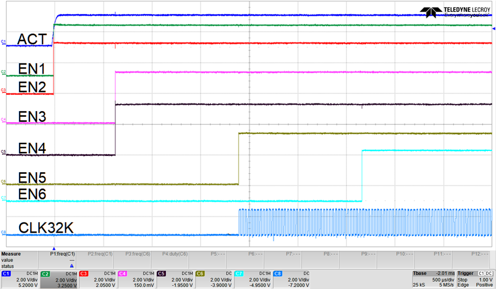 Figure 9-2 Power Up Sequence
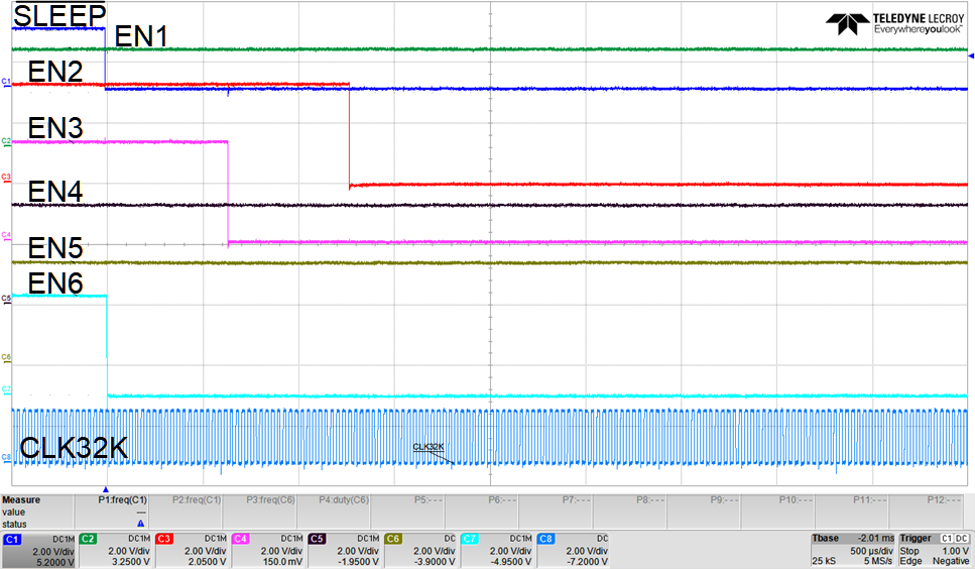 Figure 9-4 Sleep Entry Sequence
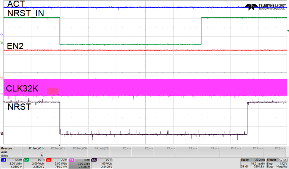 Figure 9-6 RESET Triggered by NRST_IN
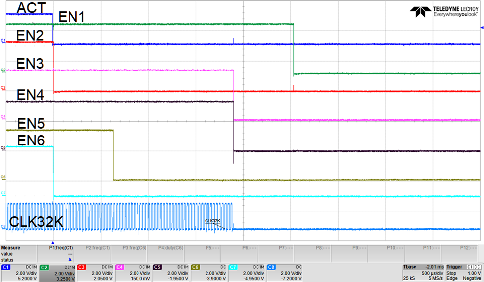 Figure 9-3 Power Down Sequence
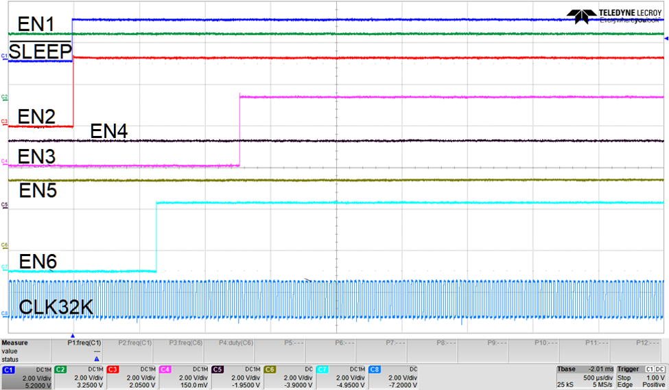 Figure 9-5 Sleep Exit Sequence
Figure 9-2 depicts the power up sequencing order listed in Table 9-1. Notice EN1 rises at the same time as the ACT signal due to the number 1 slot selection. Additonally, notice EN3 and EN4 rise 625us after EN1 due to the number two slot selection. The TPS38700-Q1 timing tool found under the "Design tool's & simulation" section of the TPS38700-Q1 web page can be used to assist in implementing a desired slot selection.