SLUS719H MARCH 2007 – May 2019 TPS40192 , TPS40193
PRODUCTION DATA.
- 1 Features
- 2 Applications
- 3 Description
- 4 Revision History
- 5 Pin Configuration and Functions
- 6 Specifications
- 7 Detailed Description
-
8 Application and Implementation
- 8.1 Application Information
- 8.2
Typical Application
- 8.2.1 Design Requirements
- 8.2.2
Detailed Design Procedure
- 8.2.2.1 Selecting the Switching Frequency
- 8.2.2.2 Inductor Selection
- 8.2.2.3 Output Capacitor Selection (C8)
- 8.2.2.4 Peak Current Rating of the Inductor
- 8.2.2.5 Input Capacitor Selection (C7)
- 8.2.2.6 MOSFET Switch Selection (Q1, Q2)
- 8.2.2.7 Boot Strap Capacitor
- 8.2.2.8 Input Bypass Capacitor (C6)
- 8.2.2.9 BP5 Bypass Capacitor (C5)
- 8.2.2.10 Input Voltage Filter Resistor (R11)
- 8.2.2.11 Short Circuit Protection (R9)
- 8.2.2.12 Feedback Compensation (Modeling the Power Stage)
- 8.2.2.13 Feedback Divider (R7, R8)
- 8.2.2.14 Error Amplifier Compensation (R6, R10, C1, C2, C3)
- 8.2.3 Application Curves
- 9 Power Supply Recommendations
- 10Layout
- 11Device and Documentation Support
- 12Mechanical, Packaging, and Orderable Information
Package Options
Mechanical Data (Package|Pins)
- DRC|10
Thermal pad, mechanical data (Package|Pins)
- DRC|10
Orderable Information
8.2.2.14 Error Amplifier Compensation (R6, R10, C1, C2, C3)
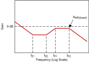
Place two zeros at 50% and 100% of the resonance frequency to boost the phase margin before resonance frequency generates –180° of phase shift. For fRES = 11.7 kHz, fZ1 = 5.8 kHz and fZ2 = 11 kHz. Selecting the crossover frequency (fCO) of the control loop between 3 times the LC filter resonance and 1/5th the switching frequency. For most applications 1/10th the switching frequency provides a good balance between ease of design and fast transient response.
- If fESR < fCO ; fP1 = fESR and fP2 = 4 × fCO
- If fESR > 2 × fCO; fP1 = fCO and fP2 = 8 × fCO.
- fSW = 600 kHz
- fRES = 11.7 kHz
- fESR = 636 kHz
- fCO = 60 kHz and because
- fESR > 2 × fCO, FP1 = fCO = 60 kHz and fP2 = 4 × fCO = 500 kHz.
For this design
Because fCO < fESR the power stage gain at the desired crossover can be approximated in Equation 31.

Table 5. Error Amplifier Design Parameters
| PARAMETER | SYMBOL | VALUE | UNITS |
|---|---|---|---|
| First zero frequency | fZ1 | 5.8 | kHz |
| Second zero frequency | fZ2 | 11.0 | |
| First pole frequency | fP1 | 60 | |
| Second pole frequency | fP2 | 500 | |
| Midband gain | AMID(band) | 1.86 | V/V |
Approximate C2 with the formula described in Equation 32.

For a calculated value for C2 of 723 pF, the closest standard capacitor value is 1000 pF.
Approximate R10 using Equation 33.

For a calculated value for R10 of 2.65 kΩ, the closest standard resistor value is 2.61 kΩ.
Calculate R6 using Equation 34.

For a calculated value for R6 of 4.29 kΩ, the closest standard resistor value is 4.22 kΩ.
Calculate C1 and C3 using Equation 35 and Equation 36.


Using the a standard value close to 75 pF, select C1 = 100 pF. Likewise, using a standard value close to 6.5 nF, select C3 = 10 nF.
The error amplifier straight line approximation transfer function is described in Figure 18.
 Figure 18. Error Amplifier Transfer Function Approximation