SLUS719H MARCH 2007 – May 2019 TPS40192 , TPS40193
PRODUCTION DATA.
- 1 Features
- 2 Applications
- 3 Description
- 4 Revision History
- 5 Pin Configuration and Functions
- 6 Specifications
- 7 Detailed Description
-
8 Application and Implementation
- 8.1 Application Information
- 8.2
Typical Application
- 8.2.1 Design Requirements
- 8.2.2
Detailed Design Procedure
- 8.2.2.1 Selecting the Switching Frequency
- 8.2.2.2 Inductor Selection
- 8.2.2.3 Output Capacitor Selection (C8)
- 8.2.2.4 Peak Current Rating of the Inductor
- 8.2.2.5 Input Capacitor Selection (C7)
- 8.2.2.6 MOSFET Switch Selection (Q1, Q2)
- 8.2.2.7 Boot Strap Capacitor
- 8.2.2.8 Input Bypass Capacitor (C6)
- 8.2.2.9 BP5 Bypass Capacitor (C5)
- 8.2.2.10 Input Voltage Filter Resistor (R11)
- 8.2.2.11 Short Circuit Protection (R9)
- 8.2.2.12 Feedback Compensation (Modeling the Power Stage)
- 8.2.2.13 Feedback Divider (R7, R8)
- 8.2.2.14 Error Amplifier Compensation (R6, R10, C1, C2, C3)
- 8.2.3 Application Curves
- 9 Power Supply Recommendations
- 10Layout
- 11Device and Documentation Support
- 12Mechanical, Packaging, and Orderable Information
Package Options
Mechanical Data (Package|Pins)
- DRC|10
Thermal pad, mechanical data (Package|Pins)
- DRC|10
Orderable Information
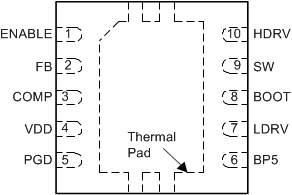
5 Pin Configuration and Functions
Pin Functions
| PIN | I/O | DESCRIPTION | |
|---|---|---|---|
| NAME | NO. | ||
| BOOT | 8 | I | Gate drive voltage for the high-side N-channel MOSFET. A 100-nF typical capacitor must be connected between this pin and SW. |
| BP5 | 6 | O | Output bypass for the internal regulator. Connect a capacitor with a value of at least 1-μF from this pin to GND. Larger capacitors (up to 4.7 μF) can improve noise performance when using a low-side MOSFET with a gate charge of 25 nC or greater. Low power, low noise loads may be connected here if desired. The sum of the external load and the gate drive requirements must not exceed 50 mA. This regulator is turned off when ENABLE is pulled low. |
| COMP | 3 | O | Output of the error amplifier. |
| ENABLE | 1 | I | Logic level input which starts or stops the controller from an external user command. A high-level turns the controller on. A weak internal pullup holds this pin high so that the pin may be left floating if this function is not used. |
| FB | 2 | I | Inverting input to the error amplifier. In normal operation the voltage on this pin is equal to the internal reference voltage (591 mV typical) |
| HDRV | 10 | O | Bootstrapped output for driving the gate of the high-side N-channel FET. |
| LDRV | 7 | O | Output to the rectifier MOSFET gate |
| PGD | 5 | O | Open drain power good output |
| SW | 9 | I | Sense line for the adaptive anti-cross conduction circuitry. Serves as common connection for the flying high-side MOSFET driver |
| VDD | 4 | I | Power input to the controller |
| Thermal pad | G | Common reference for the device. Connect to the system GND. | |
