SLVS861F august 2008 – june 2020 TPS40210-Q1 , TPS40211-Q1
PRODUCTION DATA
- 1 Features
- 2 Applications
- 3 Description
- 4 Revision History
- 5 Pin Configuration and Functions
- 6 Specifications
-
7 Detailed Description
- 7.1 Overview
- 7.2 Functional Block Diagram
- 7.3
Feature Description
- 7.3.1 Minimum On-Time and Off-Time Considerations
- 7.3.2 Current Sense and Overcurrent
- 7.3.3 Current Sense and Subharmonic Instability
- 7.3.4 Current Sense Filtering
- 7.3.5 Soft Start
- 7.3.6 BP Regulator
- 7.3.7 Shutdown (DIS/ EN Pin)
- 7.3.8 Control Loop Considerations
- 7.3.9 Gate Drive Circuit
- 7.3.10 TPS40211-Q1
- 7.4 Device Functional Modes
-
8 Application and Implementation
- 8.1 Application Information
- 8.2
Typical Application
- 8.2.1 Design Requirements
- 8.2.2
Detailed Design Procedure
- 8.2.2.1 Duty Cycle Estimation
- 8.2.2.2 Inductor Selection
- 8.2.2.3 Rectifier Diode Selection
- 8.2.2.4 Output Capacitor Selection
- 8.2.2.5 Input Capacitor Selection
- 8.2.2.6 Current Sense and Current Limit
- 8.2.2.7 Current Sense Filter
- 8.2.2.8 Switching MOSFET Selection
- 8.2.2.9 Feedback Divider Resistors
- 8.2.2.10 Error Amplifier Compensation
- 8.2.2.11 R-C Oscillator
- 8.2.2.12 Soft-Start Capacitor
- 8.2.2.13 Regulator Bypass
- 8.2.3 Application Curves
- 9 Power Supply Recommendations
- 10Layout
- 11Device and Documentation Support
- 12Mechanical, Packaging, and Orderable Information
Package Options
Refer to the PDF data sheet for device specific package drawings
Mechanical Data (Package|Pins)
- DGQ|10
Thermal pad, mechanical data (Package|Pins)
Orderable Information
7.3.10 TPS40211-Q1
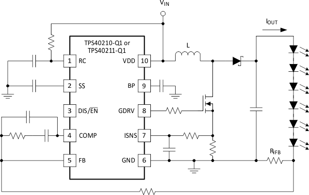
The only difference between the TPS40210-Q1 and the TPS40211-Q1 devices is the reference voltage that the error amplifier uses to regulate the output voltage. The TPS40211-Q1 device uses a 260-mV reference and is intended for applications where the output is actually a current instead of a regulated voltage. A typical example of an application of this type is an LED driver. Figure 27 shows an example schematic.
An example of an LED driver design using the TPS40211-Q1 device with detailed analysis is available in the TPS40211 – SEPIC Design for MR-16 LED Application Report.
 Figure 27. Typical LED Drive Schematic
 The current in the LED string is set by the choice of the resistor RISNS as shown in Equation 30.

where
- RIFB is the value of the current sense resistor for the LED string in Ω
- VFB is the reference voltage for the TPS40211-Q1 device in volts (0.26 V typ)
- IOUT is the desired dc current in the LED string in amperes