SLUS772G March 2008 – June 2020 TPS40210 , TPS40211
PRODUCTION DATA
- 1 Features
- 2 Applications
- 3 Description
- 4 Revision History
- 5 Pin Configuration and Functions
- 6 Specifications
-
7 Detailed Description
- 7.1 Overview
- 7.2 Functional Block Diagram
- 7.3
Feature Description
- 7.3.1 Soft Start
- 7.3.2 BP Regulator
- 7.3.3 Shutdown (DIS/ EN Pin)
- 7.3.4 Minimum On-Time and Off-Time Considerations
- 7.3.5 Setting the Oscillator Frequency
- 7.3.6 Synchronizing the Oscillator
- 7.3.7 Current Sense and Overcurrent
- 7.3.8 Current Sense and Subharmonic Instability
- 7.3.9 Current Sense Filtering
- 7.3.10 Control Loop Considerations
- 7.3.11 Gate Drive Circuit
- 7.3.12 TPS40211
- 7.4 Device Functional Modes
-
8 Application and Implementation
- 8.1 Application Information
- 8.2
Typical Applications
- 8.2.1
12-V to 24-V Nonsynchronous Boost Regulator
- 8.2.1.1 Design Requirements
- 8.2.1.2
Detailed Design Procedure
- 8.2.1.2.1 Custom Design with WEBENCH Tools
- 8.2.1.2.2 Duty Cycle Estimation
- 8.2.1.2.3 Inductor Selection
- 8.2.1.2.4 Rectifier Diode Selection
- 8.2.1.2.5 Output Capacitor Selection
- 8.2.1.2.6 Input Capacitor Selection
- 8.2.1.2.7 Current Sense and Current Limit
- 8.2.1.2.8 Current Sense Filter
- 8.2.1.2.9 Switching MOSFET Selection
- 8.2.1.2.10 Feedback Divider Resistors
- 8.2.1.2.11 Error Amplifier Compensation
- 8.2.1.2.12 RC Oscillator
- 8.2.1.2.13 Soft-Start Capacitor
- 8.2.1.2.14 Regulator Bypass
- 8.2.1.2.15 Bill of Materials
- 8.2.1.3 Application Curves
- 8.2.2 12-V Input, 700-mA LED Driver, Up to 35-V LED String
- 8.2.1
12-V to 24-V Nonsynchronous Boost Regulator
- 9 Power Supply Recommendations
- 10Layout
- 11Device and Documentation Support
- 12Mechanical, Packaging, and Orderable Information
Package Options
Refer to the PDF data sheet for device specific package drawings
Mechanical Data (Package|Pins)
- DRC|10
- DGQ|10
Thermal pad, mechanical data (Package|Pins)
Orderable Information
7.3.7 Current Sense and Overcurrent
The TPS4021x is a current mode controller that uses a resistor in series with the source terminal power FET to sense current for both the current mode control and overcurrent protection. The device enters a current limit state if the voltage on the ISNS pin exceeds the current limit threshold voltage VISNS(oc) from the Section 6.5. When this happens, the controller discharges the SS capacitor through a relatively high impedance and then attempts to restart. The amount of output current that causes this to happen is dependent on several variables in the converter.
 Figure 7-6 Oscillator Components
 Figure 7-7 Current Sense Components
The load current overcurrent threshold is set by proper choice of RISNS. If the converter is operating in discontinuous mode, the current sense resistor is found in Equation 15.
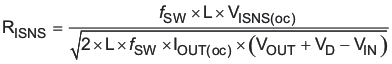
If the converter is operating in continuous conduction mode, RISNS can be found in Equation 16.
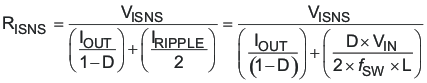
where
- RISNS is the value of the current sense resistor in Ω
- VISNS(oc) is the overcurrent threshold voltage at the ISNS pin (from electrical specifications)
- D is the duty cycle (from Equation 11)
- fSW is the switching frequency in Hz
- VIN is the input voltage to the power stage in V (see text)
- L is the value of the inductor in H
- IOUT(oc) is the desired overcurrent trip point in A
- VD is the drop across the diode in Figure 7-7
The TPS40210 and TPS40211 have a fixed undervoltage lockout (UVLO) that allows the controller to start at a typical input voltage of 4.25 V. If the input voltage is slowly rising, the converter might have less than its designed nominal input voltage available when it has reached regulation. As a result, this can decrease the apparent current limit load current value and must be taken into consideration when selecting RISNS. The value of VIN used to calculate RISNS must be the value at which the converter finishes start-up. The total converter output current at start-up is the sum of the external load current and the current required to charge the output capacitor or capacitors. See the Section 7.3.1 section of this data sheet for information on calculating the required output capacitor charging current.
The topology of the standard boost converter has no method to limit current from the input to the output in the event of a short circuit fault on the output of the converter. If protection from this type of event is desired, it is necessary to use some secondary protection scheme, such as a fuse, or rely on the current limit of the upstream power source.