SLUS964D NOVEMBER 2009 – March 2018 TPS40303 , TPS40304 , TPS40305
PRODUCTION DATA.
- 1 Features
- 2 Applications
- 3 Description
- 4 Revision History
- 5 Pin Configuration and Functions
- 6 Specifications
- 7 Detailed Description
-
8 Application and Implementation
- 8.1 Application Information
- 8.2
Typical Applications
- 8.2.1
Using the TPS40305 for a 12-V to 1.8-V Point-of-Load Synchronous Buck Regulator
- 8.2.1.1 Design Requirements
- 8.2.1.2
Detailed Design Procedure
- 8.2.1.2.1 Custom Design With WEBENCH® Tools
- 8.2.1.2.2 Selecting the Switching Frequency
- 8.2.1.2.3 Inductor Selection (L1)
- 8.2.1.2.4 Output Capacitor Selection (C12)
- 8.2.1.2.5 Peak Current Rating of Inductor
- 8.2.1.2.6 Input Capacitor Selection (C8)
- 8.2.1.2.7 MOSFET Switch Selection (Q1 and Q2)
- 8.2.1.2.8 Bootstrap Capacitor (C6)
- 8.2.1.2.9 VDD Bypass Capacitor (C7)
- 8.2.1.2.10 BP Bypass Capacitor (C5)
- 8.2.1.2.11 Short-Circuit Protection (R11)
- 8.2.1.2.12 Feedback Divider (R4, R5)
- 8.2.1.2.13 Compensation: (C2, C3, C4, R3, R6)
- 8.2.1.3 Application Curves
- 8.2.2
A High-Current, Low-Voltage Design Using the TPS40304
- 8.2.2.1 Design Requirements
- 8.2.2.2
Detailed Design Procedure
- 8.2.2.2.1 Selecting the Switching Frequency
- 8.2.2.2.2 Inductor Selection (L1)
- 8.2.2.2.3 Output Capacitor Selection (C12)
- 8.2.2.2.4 Peak Current Rating of Inductor
- 8.2.2.2.5 Input Capacitor Selection (C8)
- 8.2.2.2.6 MOSFET Switch Selection (Q1 and Q2)
- 8.2.2.2.7 Bootstrap Capacitor (C6)
- 8.2.2.2.8 VDD Bypass Capacitor (C7)
- 8.2.2.2.9 BP Bypass Capacitor (C5)
- 8.2.2.2.10 Short-Circuit Protection (R11)
- 8.2.2.2.11 Feedback Divider (R4, R5)
- 8.2.2.2.12 Compensation: (C2, C3, C4, R3, R6)
- 8.2.2.3 Application Curves
- 8.2.3
A Synchronous Buck Application Using the TPS40303
- 8.2.3.1 Design Requirements
- 8.2.3.2
Detailed Design Procedure
- 8.2.3.2.1 Selecting the Switching Frequency
- 8.2.3.2.2 Inductor Selection (L1)
- 8.2.3.2.3 Output Capacitor Selection (C12)
- 8.2.3.2.4 Peak Current Rating of Inductor
- 8.2.3.2.5 Input Capacitor Selection (C8)
- 8.2.3.2.6 MOSFET Switch Selection (Q1 and Q2)
- 8.2.3.2.7 Bootstrap Capacitor (C6)
- 8.2.3.2.8 VDD Bypass Capacitor (C7)
- 8.2.3.2.9 BP Bypass Capacitor (C5)
- 8.2.3.2.10 Short-Circuit Protection (R11)
- 8.2.3.2.11 Feedback Divider (R4, R5)
- 8.2.3.2.12 Compensation: (C2, C3, C4, R3, R6)
- 8.2.3.3 Application Curves
- 8.2.1
Using the TPS40305 for a 12-V to 1.8-V Point-of-Load Synchronous Buck Regulator
- 9 Power Supply Recommendations
- 10Layout
- 11Device and Documentation Support
- 12Mechanical, Packaging, and Orderable Information
Package Options
Mechanical Data (Package|Pins)
- DRC|10
Thermal pad, mechanical data (Package|Pins)
- DRC|10
Orderable Information
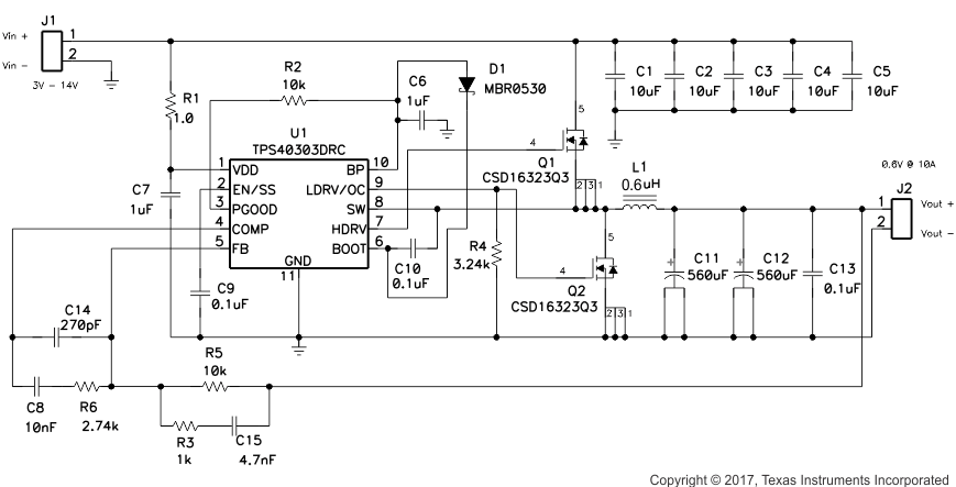
8.2.3 A Synchronous Buck Application Using the TPS40303
Figure 22 shows a 3.3-V/5-V/12-V to 0.6-V at 10-A synchronous buck application using the TPS40303 switching at 300 kHz.
 Figure 22. TPS40303 Design Example Schematic