SLVSBP4D December 2012 – September 2014 TPS43060 , TPS43061
PRODUCTION DATA.
- 1 Features
- 2 Applications
- 3 Description
- 4 Simplified Schematic
- 5 Revision History
- 6 Pin Configuration and Functions
- 7 Specifications
-
8 Detailed Description
- 8.1 Overview
- 8.2 Functional Block Diagram
- 8.3
Feature Description
- 8.3.1 Switching Frequency
- 8.3.2 Low-Dropout Regulator
- 8.3.3 Input Undervoltage (UV)
- 8.3.4 Enable and Adjustable UVLO
- 8.3.5 Voltage Reference and Setting Output Voltage
- 8.3.6 Minimum On-Time and Pulse Skipping
- 8.3.7 Zero-Cross Detection and Duty Cycle
- 8.3.8 Minimum Off-Time and Maximum Duty Cycle
- 8.3.9 Soft-Start
- 8.3.10 Power Good
- 8.3.11 Overvoltage Protection (OVP)
- 8.3.12 OVP and Current Sense Resistor Selection
- 8.3.13 Gate Drivers
- 8.3.14 Thermal Shutdown
- 8.4 Device Functional Modes
-
9 Application and Implementation
- 9.1 Application Information
- 9.2
Typical Applications
- 9.2.1
Synchronous Boost Converter Typical Application Using TPS43061
- 9.2.1.1 Design Requirements
- 9.2.1.2
Detailed Design Procedure
- 9.2.1.2.1 Selecting the Switching Frequency
- 9.2.1.2.2 Inductor Selection
- 9.2.1.2.3 Selecting the Current Sense Resistor
- 9.2.1.2.4 Output Capacitor Selection
- 9.2.1.2.5 MOSFET Selection - NexFET Power Block
- 9.2.1.2.6 Bootstrap Capacitor Selection
- 9.2.1.2.7 VCC Capacitor
- 9.2.1.2.8 Input Capacitor
- 9.2.1.2.9 Output Voltage and Feedback Resistors Selection
- 9.2.1.2.10 Setting the Soft-Start Time
- 9.2.1.2.11 UVLO Set Point
- 9.2.1.2.12 Power Good Resistor Selection
- 9.2.1.2.13 Control Loop Compensation
- 9.2.1.2.14 DCM, Pulse-Skip Mode, and No-Load Input Current
- 9.2.1.3 Application Curves
- 9.2.2 High-Efficiency 40-V Synchronous Boost Converter Typical Application Using TPS43060
- 9.2.1
Synchronous Boost Converter Typical Application Using TPS43061
- 10Power Supply Recommendations
- 11Layout
- 12Device and Documentation Support
- 13Mechanical, Packaging, and Orderable Information
Package Options
Mechanical Data (Package|Pins)
- RTE|16
Thermal pad, mechanical data (Package|Pins)
- RTE|16
Orderable Information
1 Features
- 58-V Maximum Output Voltage
- 4.5 to 38 V (40 V Absolute Max) VIN Range
- TPS43060: 7.5-V Gate Drive Optimized for Standard Threshold MOSFETs
- TPS43061: 5.5-V Gate Drive Optimized for Low Qg NexFET™ Power MOSFETs
- Current-Mode Control With Internal Slope Compensation
- Adjustable Frequency from 50 kHz to 1 MHz
- Synchronization Capability to External Clock
- Adjustable Soft-Start Time
- Inductor DCR or Resistor Current Sensing
- Output Voltage Power-Good Indicator
- ±0.8% Feedback Reference Voltage
- 5-µA Shutdown Supply Current
- 600-µA Operating Quiescent Current
- Integrated Bootstrap Diode (TPS43061)
- Cycle-by-Cycle Current Limit and Thermal Shutdown
- Adjustable Undervoltage Lockout (UVLO) and Output Overvoltage Protection
- Small 16-Pin WQFN (3 mm × 3 mm) Package With PowerPAD™
- –40°C to 150°C Operating TJ Range
2 Applications
- Thunderbolt Port for PCs
- Automotive Power Systems
- Synchronous Flyback
- GaN RF Power Amplifiers
- Tablet Computer Accessories
- Battery-Powered Systems
- 5-V, 12-V, and 24-V DC Bus Power Systems
3 Description
The TPS43060 and TPS43061 are low IQ current-mode synchronous boost controllers with wide-input voltage range from 4.5 to 38 V (40 V absolute max) and boosted output range up to 58 V. Synchronous rectification enables high-efficiency for high-current applications, and lossless inductor DCR sensing further improves efficiency. The resulting low-power losses combined with a 3-mm × 3-mm WQFN-16 package with PowerPAD™ supports high power-density and high-reliability boost converter solutions over extended (–40°C to 150°C) temperature range.
The TPS43060 includes a 7.5-V gate drive supply, which is suitable to drive a broad range of MOSFETs. The TPS43061 has a 5.5-V gate drive supply and driver strength optimized for low Qg NexFET power MOSFETs. Also, TPS43061 provides an integrated bootstrap diode for the high-side gate driver to reduce the external parts count.
Device Information(1)
| PART NUMBER | PACKAGE | BODY SIZE (NOM) |
|---|---|---|
| TPS43060 | RTE (16) | 3.00 mm × 3.00 mm |
| TPS43061 |
- For all available packages, see the orderable addendum at the end of the data sheet.
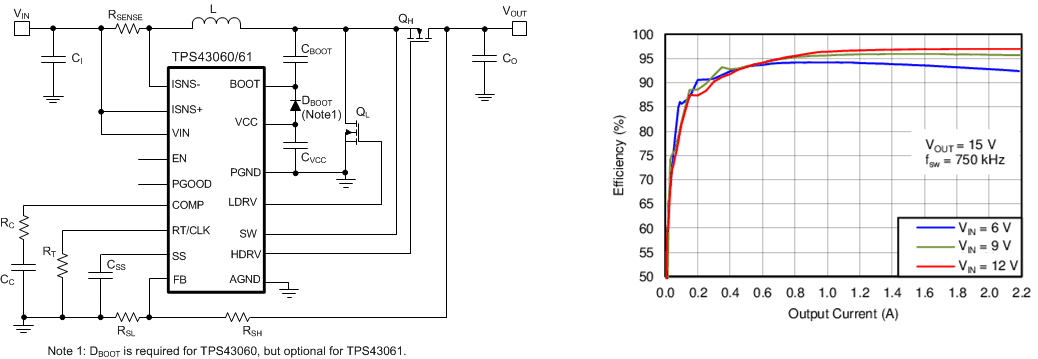
4 Simplified Schematic
