SLUSEE8 September 2022 TPS51383
PRODUCTION DATA
- 1 Features
- 2 Applications
- 3 Description
- 4 Revision History
- 5 Pin Configuration and Functions
- 6 Specifications
-
7 Detailed Description
- 7.1 Overview
- 7.2 Functional Block Diagram
- 7.3
Feature Description
- 7.3.1 PWM Operation and D-CAP3 Control Mode
- 7.3.2 VCC LDO
- 7.3.3 Soft Start
- 7.3.4 Enable Control
- 7.3.5 Power Good
- 7.3.6 Overcurrent Protection and Undervoltage Protection
- 7.3.7 100-mA LDO with Switch Over
- 7.3.8 UVLO Protection
- 7.3.9 Overvoltage Protection
- 7.3.10 Output Voltage Discharge
- 7.3.11 Thermal Shutdown
- 7.4 Device Functional Modes
- 8 Application and Implementation
- 9 Device and Documentation Support
- 10Mechanical, Packaging, and Orderable Information
Package Options
Mechanical Data (Package|Pins)
- RJN|12
Thermal pad, mechanical data (Package|Pins)
Orderable Information
8.2.2.1.3 Input Capacitor Selection
The minimum input capacitance required is given in Equation 4.
Equation 4. 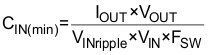
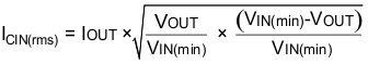
TI recommends using a high quality X5R or X7R input decoupling capacitors of 22 µF on the input voltage pin. The voltage rating on the input capacitor must be greater than the maximum input voltage. The capacitor must also have a ripple current rating greater than the maximum input current ripple of the application. The input ripple current is calculated by Equation 5 below:
Equation 5.