SLUSEE8 September 2022 TPS51383
PRODUCTION DATA
- 1 Features
- 2 Applications
- 3 Description
- 4 Revision History
- 5 Pin Configuration and Functions
- 6 Specifications
-
7 Detailed Description
- 7.1 Overview
- 7.2 Functional Block Diagram
- 7.3
Feature Description
- 7.3.1 PWM Operation and D-CAP3 Control Mode
- 7.3.2 VCC LDO
- 7.3.3 Soft Start
- 7.3.4 Enable Control
- 7.3.5 Power Good
- 7.3.6 Overcurrent Protection and Undervoltage Protection
- 7.3.7 100-mA LDO with Switch Over
- 7.3.8 UVLO Protection
- 7.3.9 Overvoltage Protection
- 7.3.10 Output Voltage Discharge
- 7.3.11 Thermal Shutdown
- 7.4 Device Functional Modes
- 8 Application and Implementation
- 9 Device and Documentation Support
- 10Mechanical, Packaging, and Orderable Information
Package Options
Mechanical Data (Package|Pins)
- RJN|12
Thermal pad, mechanical data (Package|Pins)
Orderable Information
8.2.2.1.1 Inductor Selection
The inductor ripple current is filtered by the output capacitor. A higher inductor ripple current means the output capacitor must have a ripple current rating higher than the inductor ripple current. See Table 8-2 for recommended inductor values.
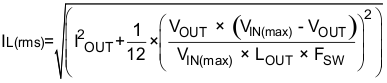
The RMS and peak currents through the inductor can be calculated using Equation 2 and Equation 3. Make sure that the inductor is rated to handle these currents.
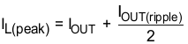
During transient, short-circuit conditions the inductor current can increase up to the current limit of the device, so choose an inductor with a saturation current higher than the peak current under current limit condition.