SLVSBF0C JULY 2012 – April 2019 TPS53015
PRODUCTION DATA.
- 1 Features
- 2 Applications
- 3 Description
- 4 Revision History
- 5 Pin Configuration and Functions
- 6 Specifications
- 7 Detailed Description
- 8 Application and Implementation
- 9 Power Supply Recommendations
- 10Layout
- 11Device and Documentation Support
- 12Mechanical, Packaging, and Orderable Information
Package Options
Mechanical Data (Package|Pins)
- DGS|10
Thermal pad, mechanical data (Package|Pins)
Orderable Information
6.6 Typical Characteristics
VIN = 12 V, TA= 25°C (unless otherwise noted)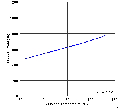 Figure 1. VIN Supply Current vs Junction Temperature
 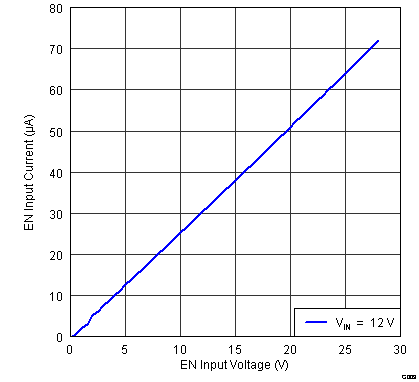 Figure 3. EN Input Current vs EN Input Voltage
 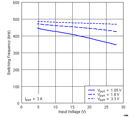 Figure 5. Switching Frequency vs Input Voltage
 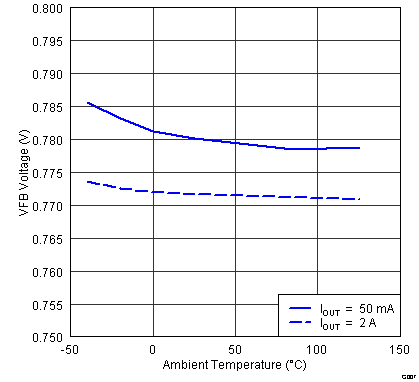 Figure 7. VFB Voltage vs Ambient Temperature
 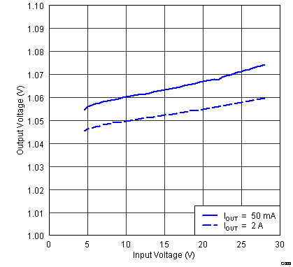 Figure 9. Line Regulation
 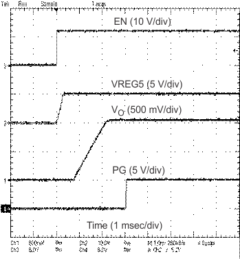 Figure 11. Start-Up Waveforms
 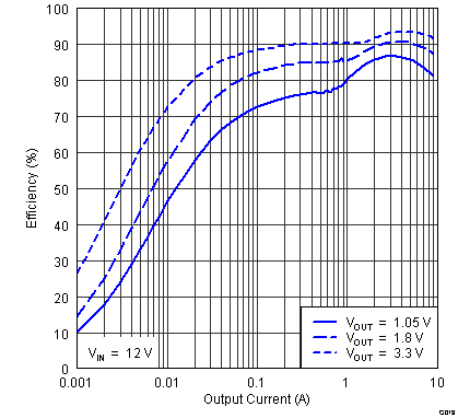 Figure 13. Light Load Efficiency vs. Output Current
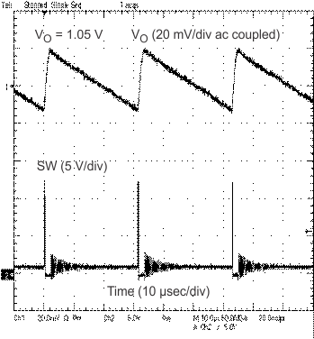
| IOUT = 50 mA |
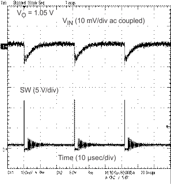
| IOUT = 50 mA |
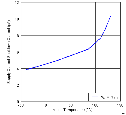 Figure 2. VIN Shutdown Current vs Junction Temperature
 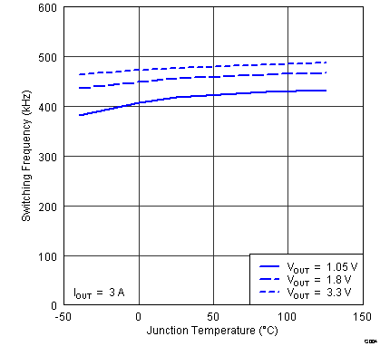 Figure 4. Switching Frequency vs Junction Temperature
 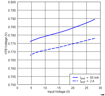 Figure 6. VFB Voltage vs Input Voltage
 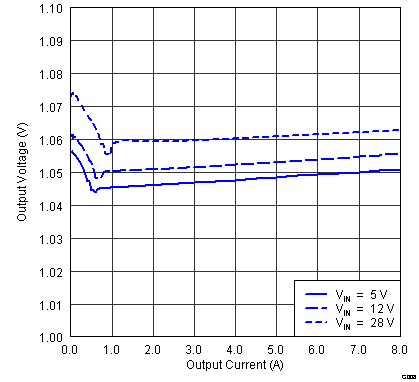 Figure 8. Load Regulation
 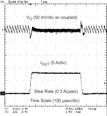 Figure 10. Transient Response
 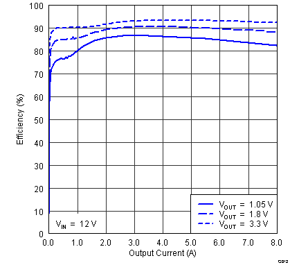 Figure 12. Efficiency vs. Output Current
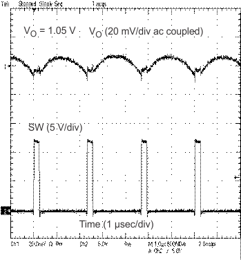
| IOUT = 8 A |
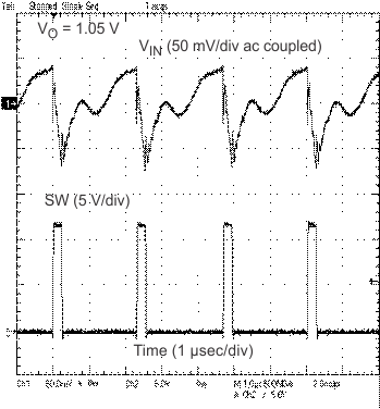
| IOUT = 8 A |