SLUSAU4B DECEMBER 2011 – February 2019 TPS53219A
PRODUCTION DATA.
- 1 Features
- 2 Applications
- 3 Description
- 4 Revision History
- 5 Pin Configuration and Functions
- 6 Specifications
-
7 Detailed Description
- 7.1 Overview
- 7.2 Functional Block Diagram
- 7.3
Feature Description
- 7.3.1 Enable and Soft-Start
- 7.3.2 Adaptive ON-Time D-CAP Control and Frequency Selection
- 7.3.3 Small Signal Model
- 7.3.4 Ramp Signal
- 7.3.5 Adaptive Zero Crossing
- 7.3.6 Output Discharge Control
- 7.3.7 Low-Side Driver
- 7.3.8 High-Side Driver
- 7.3.9 Power Good
- 7.3.10 Current Sense and Overcurrent Protection
- 7.3.11 Overvoltage and Undervoltage Protection
- 7.3.12 UVLO Protection
- 7.3.13 Thermal Shutdown
- 7.4 Device Functional Modes
- 8 Application and Implementation
- 9 Power Supply Recommendations
- 10Layout
- 11Device and Documentation Support
- 12Mechanical, Packaging, and Orderable Information
Package Options
Mechanical Data (Package|Pins)
- RGT|16
Thermal pad, mechanical data (Package|Pins)
- RGT|16
Orderable Information
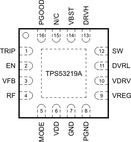
5 Pin Configuration and Functions
RGT Package
16-Pin QFN With Exposed Thermal Pad
Top View

Pin Functions
| PIN | TYPE(1) | DESCRIPTION | |
|---|---|---|---|
| NAME | NO. | ||
| DRVH | 13 | O | High-side MOSFET driver output. The SW node referenced floating driver. The gate drive voltage is defined by the voltage across VBST to SW node bootstrap flying capacitor. |
| DRVL | 11 | O | Synchronous MOSFET driver output. The PGND referenced driver. The gate drive voltage is defined by VDRV voltage. |
| EN | 2 | I | Enable pin. Place a 1-kΩ resistor in series with this pin if the source voltage is higher than 5.5 V. |
| GND | 7 | G | Ground pin. This is the ground of internal analog circuitry. Connect to GND plane at single point. |
| MODE | 5 | I | Soft-start and skip/CCM selection. Connect a resistor to select soft-start time using Table 1. The soft-start time is detected and stored into internal register during start-up. |
| NC | 15 | – | No connection. |
| PAD | – | – | Thermal pad. Use five vias to connect to GND plane. |
| PGOOD | 16 | O | Open-drain power good flag. Provides 1-ms start-up delay after the VFB pin voltage falls within specified limits. When VFB goes out specified limits PGOOD goes low after a 2-µs delay. |
| PGND | 8 | G | Power ground. Connect to GND plane. |
| RF | 4 | I | Switching frequency selection. Connect a resistor to GND or VREG to select switching frequency using Table 2. The switching frequency is detected and stored during the start-up. |
| SW | 12 | P | Output of converted power. Connect this pin to the output inductor. |
| TRIP | 1 | I | OCL detection threshold setting pin. 10 µA at room temp, 4700 ppm/°C current is sourced and set the OCL trip voltage as follows.
VOCL = VTRIP/8 spacer ( VTRIP ≤ 3 V, VOCL ≤ 375 mV) |
| VBST | 14 | P | Supply input for high-side FET gate driver (boost terminal). Connect a capacitor from this pin to SW-node. Internally connected to VREG through bootstrap MOSFET switch. |
| VDD | 6 | P | Controller power supply input. The input range is from 4.5 V to 25 V. |
| VDRV | 10 | I | Gate drive supply voltage input. Connect to VREG if using LDO output as gate drive supply. |
| VFB | 3 | I | Output feedback input. Connect this pin to VOUT through a resistor divider. |
| VREG | 9 | O | 6.2-V LDO output. This is the supply of internal analog circuitry and driver circuitry. |
(1) I=Input, O=Output, P=Power, G=Ground