SLUSAE5G August 2011 – April 2021 TPS53355
PRODUCTION DATA
- 1 Features
- 2 Applications
- 3 Description
- 4 Revision History
- 5 Pin Configuration and Functions
- 6 Specifications
-
7 Detailed Description
- 7.1 Overview
- 7.2 Functional Block Diagram
- 7.3
Feature Description
- 7.3.1 5-V LDO and VREG Start-Up
- 7.3.2 Adaptive On-Time D-CAP Control and Frequency Selection
- 7.3.3 Ramp Signal
- 7.3.4 Adaptive Zero Crossing
- 7.3.5 Power-Good
- 7.3.6 Current Sense, Overcurrent and Short Circuit Protection
- 7.3.7 Overvoltage and Undervoltage Protection
- 7.3.8 UVLO Protection
- 7.3.9 Thermal Shutdown
- 7.4 Device Functional Modes
- 8 Application and Implementation
- 9 Power Supply Recommendations
- 10Layout
- 11Device and Documentation Support
- 12Mechanical, Packaging, and Orderable Information
Package Options
Refer to the PDF data sheet for device specific package drawings
Mechanical Data (Package|Pins)
- DQP|22
Thermal pad, mechanical data (Package|Pins)
- DQP|22
Orderable Information
8.2.2.2.1 External Component Selection
Refer to Section 8.2.1.2.3 for guidelines for this design with all ceramic output capacitors.
The external components selection is a simple process when using organic semiconductors or special polymer output capacitors.
- Select operation mode and soft-start time
Select operation mode and soft-start time using Table 7-3.
- Select switching frequency
Select the switching frequency from 250 kHz to 1 MHz using Table 7-1.
- Choose the inductor
The inductance value should be determined to give the ripple current of approximately 1/4 to 1/2 of maximum output current. Larger ripple current increases output ripple voltage and improves signal-to-noise ratio and helps ensure stable operation, but increases inductor core loss. Using 1/3 ripple current to maximum output current ratio, the inductance can be determined by Equation 17.
Equation 17.
The inductor requires a low DCR to achieve good efficiency. It also requires enough room above peak inductor current before saturation. The peak inductor current can be estimated in Equation 9.
Equation 18.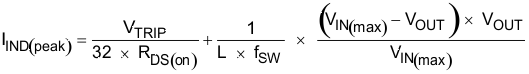
- Choose the output capacitors
When organic semiconductor capacitor(s) or specialty polymer capacitor(s) are used, for loop stability, capacitance and ESR should satisfy Equation 7. For jitter performance, Equation 19 is a good starting point to determine ESR.
Equation 19.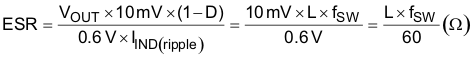
where
- D is the duty factor.
- The required output ripple slope is approximately 10 mV per tSW (switching period) in terms of VFB terminal voltage.
- Determine the value of R1 and R2
The output voltage is programmed by the voltage-divider resistor, R1 and R2 shown in Figure 8-1. R1 is connected between VFB pin and the output, and R2 is connected between the VFB pin and GND. Recommended R2 value is from 1 kΩ to 20 kΩ. Determine R1 using Equation 20.
Equation 20.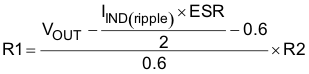
- Choose the overcurrent setting resistor
The overcurrent setting resistor, RTRIP, can be determined by Equation 10.
Equation 21.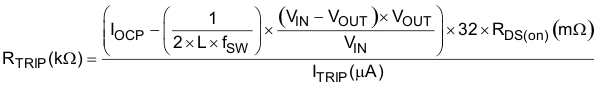
where
- ITRIP is the TRIP pin sourcing current (10 µA)
- RDS(on) is the thermally compensated on-time resistance value of the low-side MOSFET
Use an RDS(on) value of 1.5 mΩ for an overcurrent level of approximately 30 A. Use an RDS(on) value of 1.7 mΩ for overcurrent level of approximately 10 A.