SLUSBP9C SEPTEMBER   2013  – June 2018 TPS53513

PRODUCTION DATA.  

  1. Features
  2. Applications
  3. Description
    1.     Device Images
      1.      Simplified Schematic
      2.      Efficiency
  4. Revision History
  5. Pin Configuration and Functions
    1.     Pin Functions
  6. Specifications
    1. 6.1 Absolute Maximum Ratings
    2. 6.2 ESD Ratings
    3. 6.3 Recommended Operating Conditions
    4. 6.4 Thermal Information
    5. 6.5 Electrical Characteristics
    6. 6.6 Typical Characteristics
  7. Detailed Description
    1. 7.1 Overview
    2. 7.2 Functional Block Diagram
    3. 7.3 Feature Description
      1. 7.3.1  5-V LDO and VREG Start-Up
      2. 7.3.2  Enable, Soft Start, and Mode Selection
      3. 7.3.3  Frequency Selection
      4. 7.3.4  D-CAP3 Control and Mode Selection
        1. 7.3.4.1 D-CAP3 Mode
        2. 7.3.4.2 Sample and Hold Circuitry
        3. 7.3.4.3 Adaptive Zero-Crossing
      5. 7.3.5  Power-Good
      6. 7.3.6  Current Sense and Overcurrent Protection
      7. 7.3.7  Overvoltage and Undervoltage Protection
      8. 7.3.8  Out-Of-Bounds Operation
      9. 7.3.9  UVLO Protection
      10. 7.3.10 Thermal Shutdown
    4. 7.4 Device Functional Modes
      1. 7.4.1 Auto-Skip Eco-mode Light Load Operation
      2. 7.4.2 Forced Continuous-Conduction Mode
  8. Application and Implementation
    1. 8.1 Application Information
    2. 8.2 Typical Application
      1. 8.2.1 Design Requirements
      2. 8.2.2 Detailed Design Procedure
        1. 8.2.2.1 Choose the Switching Frequency
        2. 8.2.2.2 Choose the Operation Mode
        3. 8.2.2.3 Choose the Inductor
        4. 8.2.2.4 Choose the Output Capacitor
        5. 8.2.2.5 Determine the Value of R1 and R2
      3. 8.2.3 Application Curves
  9. Power Supply Recommendations
  10. 10Layout
    1. 10.1 Layout Guidelines
    2. 10.2 Layout Example
    3. 10.3 Thermal Performance
  11. 11Device and Documentation Support
    1. 11.1 Documentation Support
      1. 11.1.1 Custom Design With WEBENCH® Tools
    2. 11.2 Documentation Support
      1. 11.2.1 Related Documentation
    3. 11.3 Receiving Notification of Documentation Updates
    4. 11.4 Community Resources
    5. 11.5 Trademarks
    6. 11.6 Electrostatic Discharge Caution
    7. 11.7 Glossary
  12. 12Mechanical, Packaging, and Orderable Information

Package Options

Mechanical Data (Package|Pins)
Thermal pad, mechanical data (Package|Pins)
Orderable Information

5-V LDO and VREG Start-Up

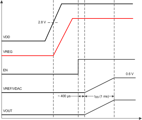
The TPS53513 device has an internal 5-V LDO feature using input from VDD and output to VREG. When the VDD voltage rises above 2.8 V, the internal LDO is enabled and outputs voltage to the VREG pin. The VREG voltage provides the bias voltage for the internal analog circuitry. The VREG voltage also provides the supply voltage for the gate drives.
TPS53513 powerup_waveforms_slusbq8.gifFigure 33. Power-up Sequence Waveforms