SNVSAZ4A February 2021 – March 2021 TPS541620
PRODUCTION DATA
- 1 Features
- 2 Applications
- 3 Description
- 4 Revision History
- 5 Pin Configuration and Functions
- 6 Specifications
-
7 Detailed Description
- 7.1 Overview
- 7.2 Functional Block Diagram
- 7.3
Feature Description
- 7.3.1 Fixed-Frequency, Internally Compensated Advanced-Current-Mode Control
- 7.3.2 Enable and UVLO
- 7.3.3 Internal LDO
- 7.3.4 Pre-biased Output Start-up
- 7.3.5 Current Sharing
- 7.3.6 Frequency Selection and Minimum On-Time and Off-Time
- 7.3.7 Ramp Compensation Selection
- 7.3.8 Soft Start
- 7.3.9 Remote Sense Function
- 7.3.10 Adjustable Output Voltage
- 7.3.11 Power Good
- 7.3.12 Overcurrent Protection
- 7.3.13 Overvoltage and Undervoltage Protection
- 7.3.14 Overtemperature Protection
- 7.3.15 Frequency Synchronization
- 7.4 Device Functional Modes
-
8 Application and Implementation
- 8.1 Application Information
- 8.2
Typical Application - Dual Independent Outputs
- 8.2.1 Design Requirements
- 8.2.2
Detailed Design Procedure
- 8.2.2.1 Switching Frequency
- 8.2.2.2 Output Inductor Selection
- 8.2.2.3 Output Capacitor
- 8.2.2.4 Input Capacitor
- 8.2.2.5 Output Voltage Resistors Selection
- 8.2.2.6 Adjustable Undervoltage Lockout
- 8.2.2.7 Bootstrap Capacitor Selection
- 8.2.2.8 BP5 Capacitor Selection
- 8.2.2.9 PGOOD Pullup Resistor
- 8.2.2.10 Current Limit
- 8.2.2.11 Soft-Start Time Selection
- 8.2.2.12 MODE1 and MODE2 Pins
- 8.2.3 Application Curves
- 8.2.4
Typical Application - 2-Phase Operation
- 8.2.4.1 Design Requirements
- 8.2.4.2
Detailed Design Procedure
- 8.2.4.2.1 Switching Frequency
- 8.2.4.2.2 Output Inductor Selection
- 8.2.4.2.3 Output Capacitor
- 8.2.4.2.4 Input Capacitor
- 8.2.4.2.5 Output Voltage Resistors Selection
- 8.2.4.2.6 Adjustable Undervoltage Lockout
- 8.2.4.2.7 Bootstrap Capacitor Selection
- 8.2.4.2.8 BP5 Capacitor Selection
- 8.2.4.2.9 PGOOD Pullup Resistor
- 8.2.4.2.10 Current Limit
- 8.2.4.2.11 Soft-Start Time Selection
- 8.2.4.2.12 MODE1 Pin
- 8.2.4.3 Application Curves
- 9 Power Supply Recommendations
- 10Layout
- 11Device and Documentation Support
- 12Mechanical, Packaging, and Orderable Information
Package Options
Mechanical Data (Package|Pins)
- RPB|25
Thermal pad, mechanical data (Package|Pins)
Orderable Information
8.2.3 Application Curves
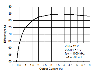 Figure 8-3 VOUT1 Efficiency
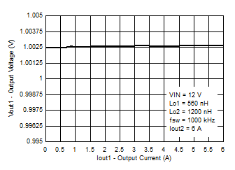 Figure 8-5 VOUT1 Load Regulation
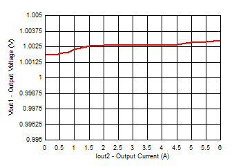 Figure 8-7 VOUT1 Cross Regulation
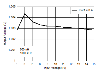 Figure 8-9 Line Regulation
VOUT1
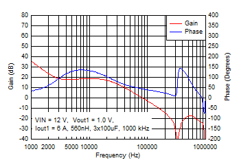 Figure 8-11 VOUT1 Bode
Plot
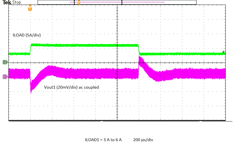 Figure 8-13 VOUT1 Load Transient
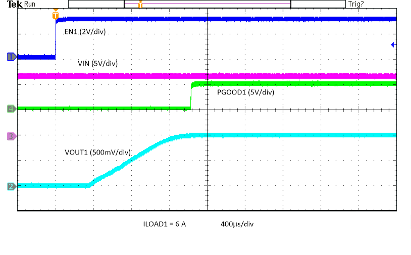 Figure 8-15 Power
Up with EN 1
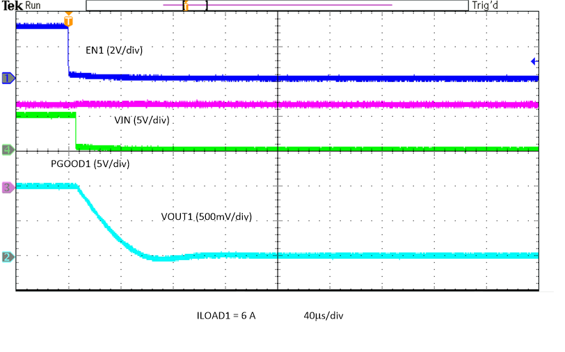 Figure 8-17 Power
Down with EN 1
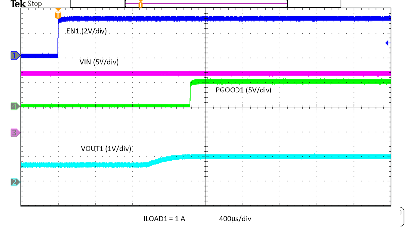 Figure 8-19 Power
Up with EN 1 with Pre Bias
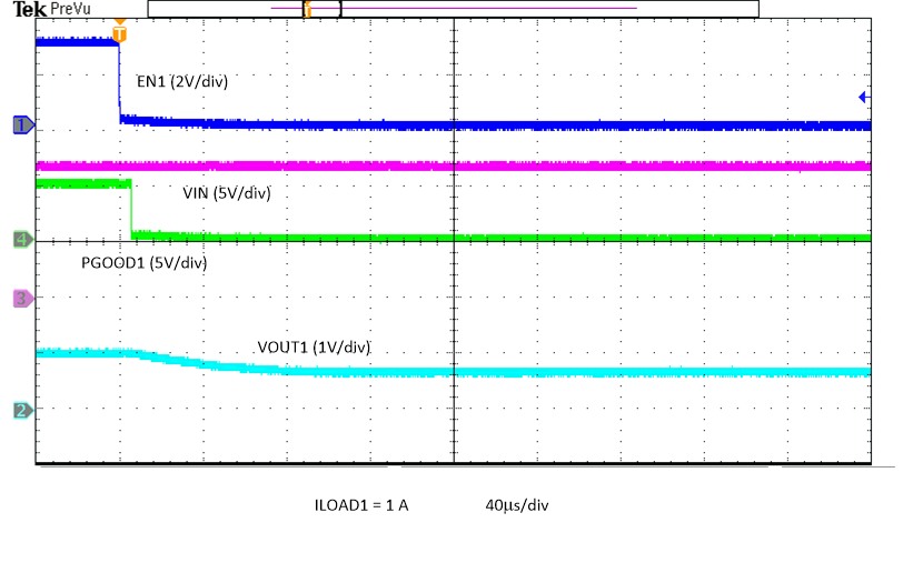 Figure 8-21 Power
Down with EN 1 with Pre Bias
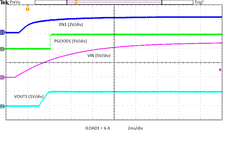 Figure 8-23 Power
Up with VIN VOUT1
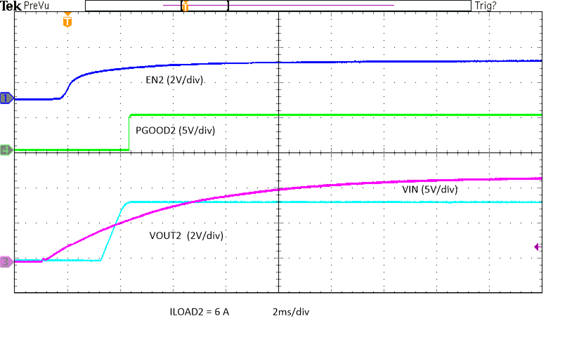 Figure 8-25 Power
Up with VIN VOUT2
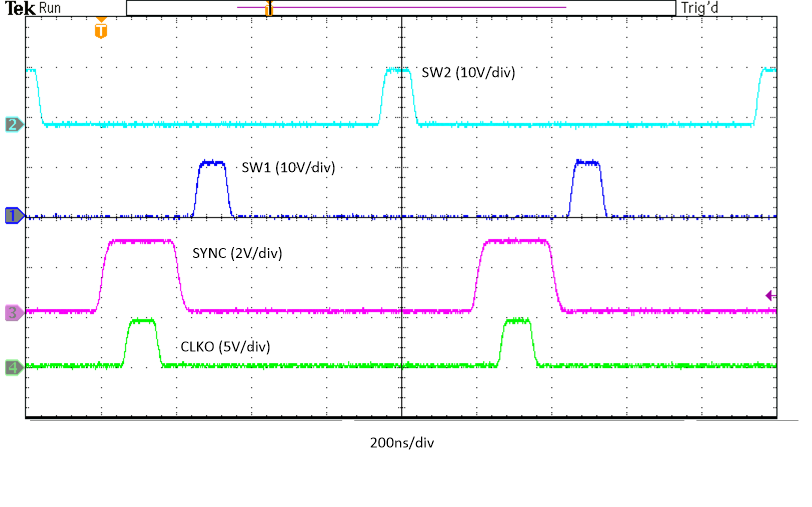 Figure 8-27 Sync
In to SW1 and SW2 Delay
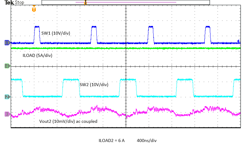 Figure 8-29 VOUT2 Output Ripple – 6-A Load
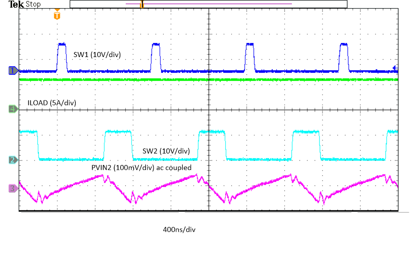 Figure 8-31 Input
Ripple PVIN2 – 6-A Load
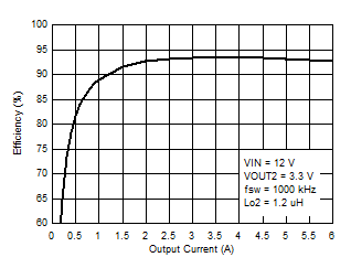 Figure 8-4 VOUT2 Efficiency
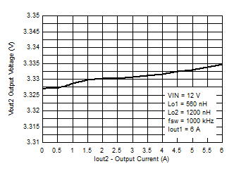 Figure 8-6 VOUT2 Load Regulation
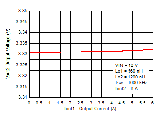 Figure 8-8 VOUT2 Cross Regulation
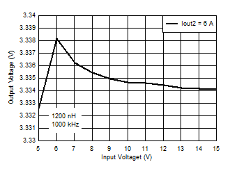 Figure 8-10 Line Regulation
VOUT2
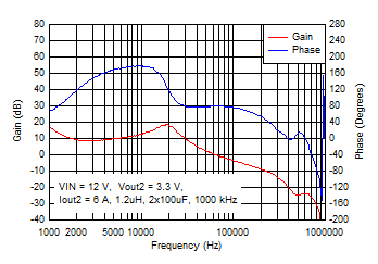 Figure 8-12 VOUT2 Bode
Plot
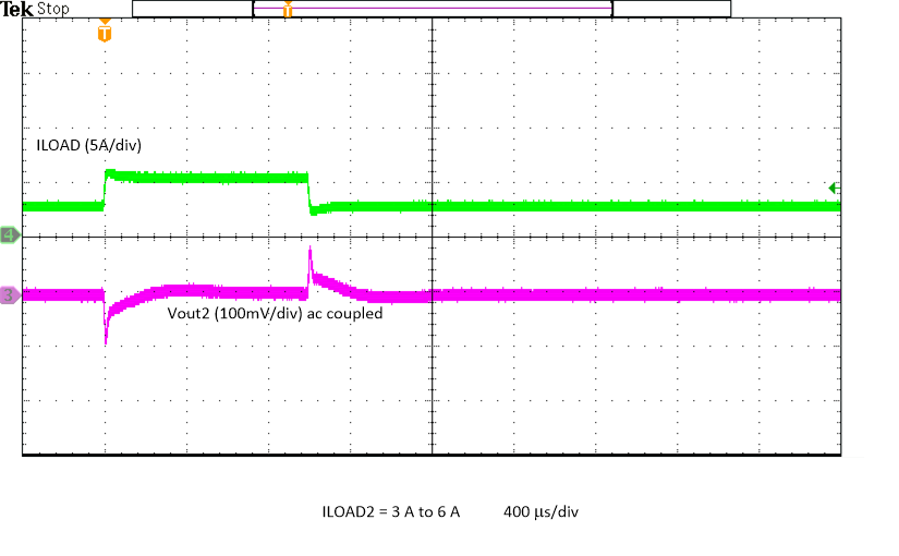 Figure 8-14 VOUT2 Load Transient
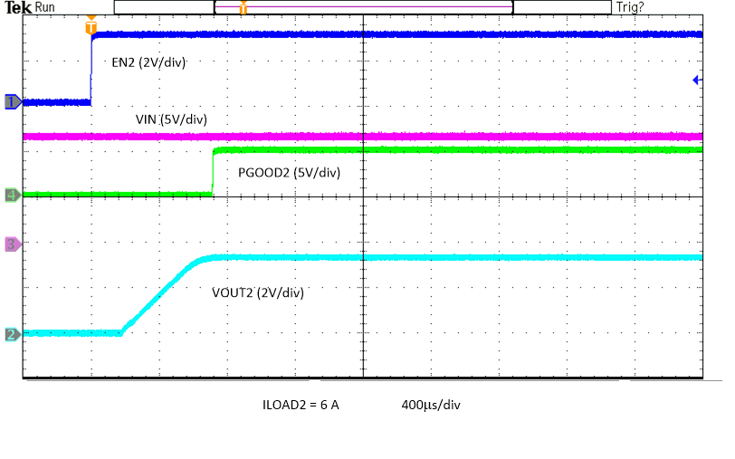 Figure 8-16 Power
Up with EN 2
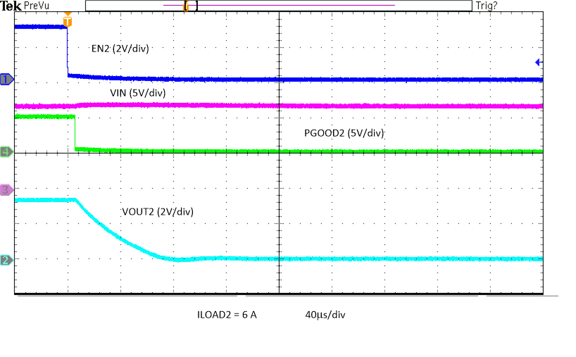 Figure 8-18 Power
Down with EN 2
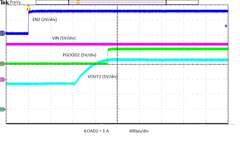 Figure 8-20 Power
Up with EN 2 with Pre Bias
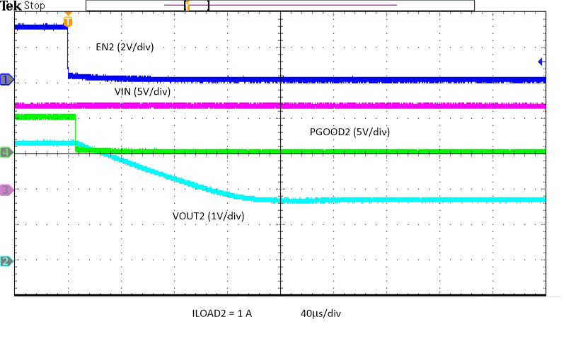 Figure 8-22 Power
Down with EN 2 with Pre Bias
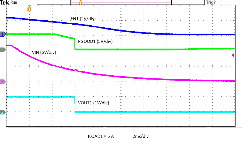 Figure 8-24 Power
Down with VIN VOUT1
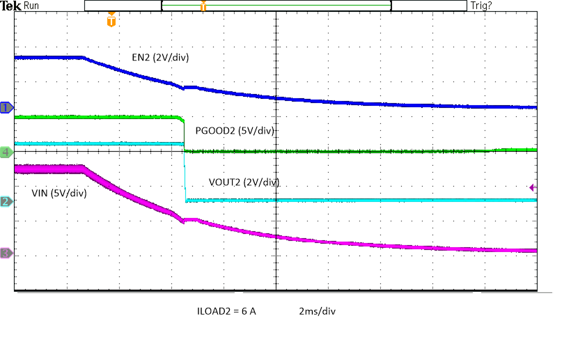 Figure 8-26 Power
Down with VIN VOUT2
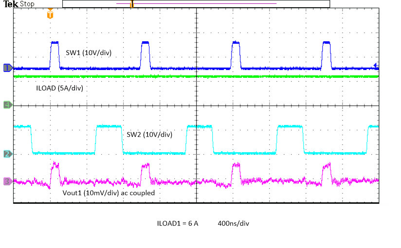 Figure 8-28 VOUT1 Output Ripple – 6-A Load
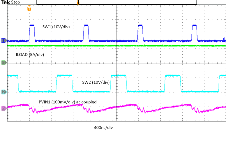 Figure 8-30 Input
Ripple PVIN1 – 6-A Load