SNVSAZ4A February 2021 – March 2021 TPS541620
PRODUCTION DATA
- 1 Features
- 2 Applications
- 3 Description
- 4 Revision History
- 5 Pin Configuration and Functions
- 6 Specifications
-
7 Detailed Description
- 7.1 Overview
- 7.2 Functional Block Diagram
- 7.3
Feature Description
- 7.3.1 Fixed-Frequency, Internally Compensated Advanced-Current-Mode Control
- 7.3.2 Enable and UVLO
- 7.3.3 Internal LDO
- 7.3.4 Pre-biased Output Start-up
- 7.3.5 Current Sharing
- 7.3.6 Frequency Selection and Minimum On-Time and Off-Time
- 7.3.7 Ramp Compensation Selection
- 7.3.8 Soft Start
- 7.3.9 Remote Sense Function
- 7.3.10 Adjustable Output Voltage
- 7.3.11 Power Good
- 7.3.12 Overcurrent Protection
- 7.3.13 Overvoltage and Undervoltage Protection
- 7.3.14 Overtemperature Protection
- 7.3.15 Frequency Synchronization
- 7.4 Device Functional Modes
-
8 Application and Implementation
- 8.1 Application Information
- 8.2
Typical Application - Dual Independent Outputs
- 8.2.1 Design Requirements
- 8.2.2
Detailed Design Procedure
- 8.2.2.1 Switching Frequency
- 8.2.2.2 Output Inductor Selection
- 8.2.2.3 Output Capacitor
- 8.2.2.4 Input Capacitor
- 8.2.2.5 Output Voltage Resistors Selection
- 8.2.2.6 Adjustable Undervoltage Lockout
- 8.2.2.7 Bootstrap Capacitor Selection
- 8.2.2.8 BP5 Capacitor Selection
- 8.2.2.9 PGOOD Pullup Resistor
- 8.2.2.10 Current Limit
- 8.2.2.11 Soft-Start Time Selection
- 8.2.2.12 MODE1 and MODE2 Pins
- 8.2.3 Application Curves
- 8.2.4
Typical Application - 2-Phase Operation
- 8.2.4.1 Design Requirements
- 8.2.4.2
Detailed Design Procedure
- 8.2.4.2.1 Switching Frequency
- 8.2.4.2.2 Output Inductor Selection
- 8.2.4.2.3 Output Capacitor
- 8.2.4.2.4 Input Capacitor
- 8.2.4.2.5 Output Voltage Resistors Selection
- 8.2.4.2.6 Adjustable Undervoltage Lockout
- 8.2.4.2.7 Bootstrap Capacitor Selection
- 8.2.4.2.8 BP5 Capacitor Selection
- 8.2.4.2.9 PGOOD Pullup Resistor
- 8.2.4.2.10 Current Limit
- 8.2.4.2.11 Soft-Start Time Selection
- 8.2.4.2.12 MODE1 Pin
- 8.2.4.3 Application Curves
- 9 Power Supply Recommendations
- 10Layout
- 11Device and Documentation Support
- 12Mechanical, Packaging, and Orderable Information
Package Options
Mechanical Data (Package|Pins)
- RPB|25
Thermal pad, mechanical data (Package|Pins)
Orderable Information
8.2.4.2.3 Output Capacitor
The two primary considerations for selecting the value of the output capacitor are how the regulator responds to a large change in load current and the output voltage ripple. The third consideration is to ensure converter stability, which is typically met from the first two considerations. The output capacitance needs to be selected based on the more stringent of these criteria.
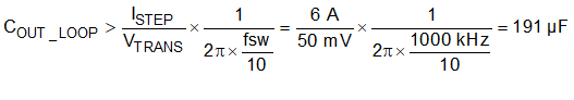
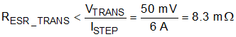
The desired response to a large change in the load current is the first criteria and is typically the most stringent. A regulator does not respond immediately to a large, fast increase or decrease in load current. The output capacitor supplies or absorbs charge until the regulator responds to the load step. The control loop needs to sense the change in the output voltage, then adjust the peak switch current in response to the change in load. The minimum output capacitance is selected based on an estimate of the loop bandwidth. Typically, the loop bandwidth is near fSW/10. Equation 28 estimates the minimum output capacitance necessary, where ISTEP is the change in output current and VTRANS is the allowable change in the output voltage.
For this example, the transient load response is specified as a 5% change in VOUT for a load step of 6 A. Therefore, ITRANS is 6 A and VTRANS is 50 mV. Using this target gives a minimum capacitance of 191 μF. This value does not take the ESR of the output capacitor into account in the output voltage change. For ceramic capacitors, the effect of the ESR can be small enough to be ignored. Aluminum electrolytic and tantalum capacitors have higher ESR that must be considered for load step response.
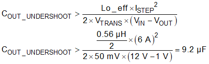
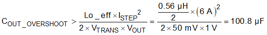
In addition to the loop bandwidth, it is possible for the inductor current slew rate to limit how quickly the regulator responds to the load step. For low duty cycle applications, the time it takes for the inductor current to ramp down after a load step down can be the limiting factor. Equation 29 estimates the minimum output capacitance necessary to limit the undershoot of the output voltage after a load step-up. Using the 0.56-µH inductance selected gives a minimum capacitance of 9.2 µF to meet to undershoot requirement. Equation 30 estimates the minimum output capacitance necessary to limit the overshoot of the output voltage after a load step down. Using the 0.56-μH inductance selected gives a minimum capacitance of 100.8 μF to meet the overshoot requirement.
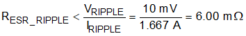
Equation 31 calculates the minimum output capacitance needed to meet the output voltage ripple specification, where fsw is the switching frequency, VRIPPLE is the maximum allowable steady-state output voltage ripple, N is the number of phases, and IRIPPLE is the inductor ripple current calculated from Equation 25. In this case, the target maximum steady-state output voltage ripple is 10 mV. Under this requirement, Equation 31 yields 10.4 µF.

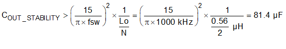
Lastly, if an application does not have a stringent load transient response or output ripple requirement, a minimum amount of capacitance is still required to ensure the control loop is stable with the lowest gain ramp setting on the MODE pin. Equation 32 estimates the minimum capacitance needed for loop stability. This equation sets the minimum amount of capacitance by keeping the LC frequency at a maximum of 1/30th the switching frequency. Equation 32 gives a minimum capacitance of 81.4 µF.
Equation 33 calculates the maximum combined ESR the output capacitors can have to meet the output voltage ripple specification, showing the ESR should be less than 6 mΩ. This application uses all ceramic capacitors, so the effects of ESR on the ripple and transient were ignored. If you are using non-ceramic capacitors, as a starting point, the ESR should be below the values calculated in Equation 33 and Equation 34, respectively, to meet the ripple and transient requirements. For more accurate calculations or if using mixed output capacitors, the impedance of the output capacitors must be used to determine if the ripple and transient requirements can be met.
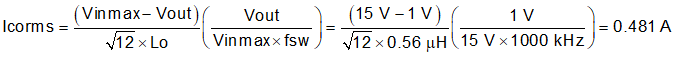
In this case, ceramic capacitors are used and the combined ESR of the ceramic capacitors in parallel is much less than is needed to meet the ripple. Capacitors also have limits to the amount of ripple current they can handle without producing excess heat and failing. An output capacitor that can support the inductor ripple current must be specified. The capacitor data sheet specifies the RMS value of the maximum ripple current. Equation 35 can be used to calculate the RMS ripple current the output capacitor needs to support. For this application, Equation 35 yields 0.481 A, and ceramic capacitors typically have a ripple current rating much higher than this. Select X5R and X7R ceramic dielectrics or equivalent for power regulator capacitors because they have a high capacitance-to-volume ratio and are fairly stable over temperature. The output capacitor must also be selected with the DC bias and AC voltage derating taken into account. The derated capacitance value of a ceramic capacitor due to DC voltage bias and AC RMS voltage is usually found on the capacitor manufacturer's website. For this application example, six 100-μF, 6.3-V, X7S, 0805 ceramic capacitors, each with 2 mΩ of ESR, are used. With the six parallel capacitors, the estimated effective output capacitance after derating using the capacitor manufacturer’s website is 240 μF. This is well above the calculated minimum capacitance, so this design is expected to meet the transient response requirement with added margin. Figure 8-38 shows the transient response. The output voltage stays within ±3%, below the ±5% target.